This thread has been locked.

If you have a related question, please click the "Ask a related question" button in the top right corner. The newly created question will be automatically linked to this question.

ADS1231 Gain Error specification

Other Parts Discussed in Thread: ADS1231, ADS1220, ADS1231REF

Hi

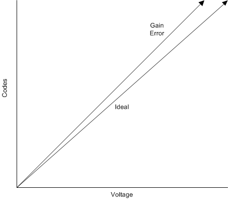
On the page 3 of the ADS1231 datasheet is a Gain Error of 1% at +25°C specified.

But in figure 8 (on page 8) I read that the Gain Error is smaller than 0.001% at 25°C. And over the whole temperature range from -40 to +85°C better than +/- 0.2%

So what is correct?

  • Hi Manuel,

    Figure 8 should be labeled Gain Drift Error.  It is similar to Figure 7 for offset drift.  Both figures are normalized for 25 deg C by showing a zero crossing at that point.  For example, if you have a gain error of 1% (the typical value shown on page 3) then across temperature for the device you would see approximately +/-0.015 % from the total gain error at room temperature for the ADS1231.  In this example you would see gain error of 1 +/- 0.015 % over the operating temperature of the part.

    Best regards,

    Bob B

  • Hi Bob
    Thanks for the clarification. Unfortunately it makes the device much less accurate than I thought it would be...
    So what does a "typical" Gain Error of 1% mean? When I buy 100pc ADS1231, how many will be within 1%? What is the worst Gain Error (at 25°C) to expect?
    I actually tested two pieces and it looks like both units have output values which are almost 4% too high (tested at 1.1mV/V and 2.1mV/V). Is this still inside the specifications? Or must there be an error somewhere?

  • Hi Manuel,

    4% is more than double I would expect worst case.  How are you determining the error?  Can you send me your current schematic?  Are you using an actual load cell with the excitation the same as the reference voltage?  If there is any excitation loss due to resistance in the leads for excitation, then you may have error you are not accounting for in the circuit path.

    Thanks,

    Bob B

  • Hi Bob

    Yes, I'm using an actual load cell (Variohm AL6N-C3-10kg-3B6).

    I've put 5703 and 10412 grams load on it and measured the output in mV/V using a dedicated wheatstone measuring device, a Campbell CR1000 datalogger and and a Fluke 287. All three units gave the same results (within 0.1% of each other). The values of the two ADS1231 units were both about 3.7% higher at both loads.

    The leads for excitation are short (maybe 1m) and are the same for all instruments. All readings were made in 4-wire configuration, no external excitation sense.

    Yes, the excitation is the same as the reference voltage.

    Actually I don't have the schematic (the circuit was biult by an external company). But I will ask them for it and post it when/if I receive it.

    Best regards

    Manuel

  • Hi Bob

    I got the schematic, see below. Is there something suspicious?

  • Hi Manuel,

    Do you have bypass/decoupling caps on your supplies?  Is there any input filtering?  Are you using a prototyping system, and if so, can you send me pictures of your setup?  If there is a dedicated PCB, can you share your layout/gerber files?

    How are you determining the gain error?  Are you using a calibrated weight?  Have you taken into account any offset?

    Best regards,

    Bob B

  • Hi Manuel,

    Maybe I should be a bit more specific.  What is the exact process steps that you are using to determine the gain error? For the three external measurements, are they just to determine the values of the weights? 

    The load cell has some error too, so one approach is to calibrate your system first, and then determine the linearity over the load cell range.  The gain error really should play little effect when the system is calibrated.  The calculation from codes to weight is determined by removing the offset and multiplying by the gain slope determined by the method used in calibration.

    If you are not planning on calibration of your system, you must still remove any offset from the measurement.  Both the load cell and the ADS1231 has offset which must be removed from the measurement.  This is the zero or unloaded scale measurement and can be either a positive or negative offset and must be removed from every measurement taken.  The ADS1231 has no internal offset calibration.

    Best regards,

    Bob B

  • Hi Bob

    In reply to your last post:

    I put the weights on the load cell and read the raw mv/V output with three precision instruments. So neigther the weights nor the load cell has to be precise, they must only produce a stable output for as long as I take the readings with the different instruments.

    I do this procedure to the check the accuracy of the ads1231 only. I don't want to calibrate a whole system (a/d with load cell). The ads1231 board should be capable to work with any load cell. The mV/V read by the ads1231 will be processed using the calibration factors supplied by the load cell manufacturer to get the actual load. I'm aware that individual calibration of each system (a/d and load cell) would be more precise, but for our application this is not feasible.

    The ads1231 input Offset specification is typically 10uV. Using 3V excitation results in 0.003mV/V offset error. Using a load cell with FS output of 1.5mV/V means that the offset error is about 0.2% of load cell range. This isn't perfect, but would work for most of our applications.

    The typical Gain error is much more a problem. 1% equals directly  to 1% errror in the calculated load. 5 times of the error introduced by the offset. And a gain error of 3.7% (as on our prototype) is even worse. I hope that the gain error is smaller than stated in the specs, maybe 0.5%. That would make the thing working for our application without any calibration. Otherwise we have eighther to calibrate each adc board or we have to search for another adc which provides better accuracy (precisier gain and lower offset) off the shelf. Would there be an alternative  from TI (single channel, very low sample rate, low power, easy digital interface, minimun input range 2mV/V, repectively 7.5mV)?

    I'll reply to your other post later.

    Best regards

    Manuel

  • Hi Manuel,

    I'm still confused about a few things.  One is with respect to the values you are giving as they don't match the load cell part number you gave me previously.  Right now that doesn't matter a lot.  What does matter is that you are using calibrated instruments and then matching them up with an non-calibrated system.  You still have not explained to me how you are calculating the 4% gain error.  As the output data of the ADS1231 is in codes relative to a voltage value, then you must know what the voltage value is if you are going to determine the gain error when comparing the result to the previous measurements you have made with the other instruments.

    One code (or LSB) = (+/- VREF/2)/128/(2^24-1) = VREF/128/(2^24-1)

    Measured voltage = #ADC codes returned * value of one code

    As an example, you will get a much different voltage result if VREF is actually 3.085V as compared to 3.0V and you use 3.0V for the calculation.

    If you want to take a look at another device you could look into the ADS1220.

    Best regards,

    Bob B

  • Hello Bob,

    I am Manuel colleague.

    Concerning the circuit: 

    there are no decoupling caps on the specific supply lines for the ADS1231, even though there are for the other components on the same PCB.

    We did not apply any input filtering on the AINN and AINP

    The system is actually is on a dedicated PCB, we can show you the part of the PCB which has the ADS1231.

    The PIN 1 of the ADS1231 is closer to the PAD named Ain+.

    Hope this made the picture clearer 

    Regards

    louis.h 

  • Hello Bob,

    I Think Manuel would like to have a system which does not need calibration as the system will be delivered to an end user who will use his own load cell.
    I guess in this case the ADS1231 is not the right choice (?)

    On another hand if the ADS1231 is to be used I would like to know if the following is a correct calibration procedure (of course for a specific load cell)

    1+ Connect the load cell to the circuit with the ADS1231
    2+ collect the reading with no load mounted on the load cell
    3+ collect the reading with a known load (preferably with a high precision tool)
    4+ now we are ready to do other measurements based on the following formula :
    Weight-to-Measure = [code(Weight-to-Measure) - code (no-load)]* Calibration-Weight (used in point 3 above) / code(calibration-weight collected in point 3 above)

    With this we should be able to measure not only positive weights but also negative (i.e. strain/stress forces)

    Best Regards
    louis.h
  • Hi Bob

    Thanks for your patience in helping me.

    The Variohm AL6N-C3-10kg-3B6 has a nominal full scale output of 2mV/V. My cell came with a calibration sheet stating that it has an output of 1.965mV/V at full scale (10 kilograms). But as you say, right know it doesn't matter a lot.

    I've calculated the 4% (in fact it is 3.7%) gain error that way:

    (Actual reading -Correct value)/Correct value * 100.

    The values measured by CR1000 were defined as to be the correct (reference) ones. But also the values from the Fluke or NewLeonardo could have been taken. It would not change much on the error calculation.

    The errors at 5421gr and 10130gr are almost identical, but the ones for 0gr are a bit different. I think this comes from the  zero offset of the instruments, which have a significant percental impact when readings are small. But negligibly influence at higher readings.

    Additionally we see that the load cell has a zero offset of about 0.65mV/V. The spreadsheet is added below:

    Error Calculation.xlsx

    I looked at the ADS1220 datasheet. Seems it has much smaller gain errror and the ability for offset calibration. Plus integrated precision temperature sensor (which might be useful for us too at one time). But the more feature, the higher is the complexity and interface. (And we don't really have time to start from scratch...)


    I hope my calculations are more clear now. I know it might not be scientifically correct, meaning that not all influences are taken in account. But I hope you can agree with the basic meaning.

    Do you think it is possible to achive much better results using the ADS1231 than we have now? Lets say below 0.5% error without calibrate each board?


    Best regards

    Manuel

  • Hi Louis,

    Creating a system that requires no calibration is not a trivial task.  All analog supply sources and components must have a very restrictive tolerance to be able measure within a specified design limit.  As the ADS1231 does not measure with respect to a weight, but rather a voltage reference, the reference source voltage is critical to the outcome.  A two point calibration in the way that you have mentioned removes the calculation of voltage from the equation and relates the outcome of result codes directly to calibrated weight value.

    Your calculation is almost correct except your divisor should include the zero load offset to get the correct gain slope and remove the codes for offset:

    Weight-to-Measure = [code(Weight-to-Measure) - code (no-load)]* Calibration-Weight (used in point 3 above) / [code(calibration-weight collected in point 3 above) - code (no-load in point 2)]

    The calibration will only be as good as the ability to overcome any noise in the calibration, so the calibrated weight should be as large as practical to create a good deflection with the load cell output.

    More information regarding the two point calibration is given in the ADS1231REF user's guide on page 8 and also includes TARE in the computation.

    Best regards,

    Bob B

  • Hi Manuel,

    It is not unreasonable to have a voltage source differ by +/-2% of the nominal value.  That was what I was trying to show before in that the reference voltage value directly corresponds to the resultant code.

    Normally a gain error shows up as a projection of divergence from the ideal.

    In this gain error case you see an increasing difference from the ideal value to the measured value getting worse as you increase the weight on the load cell.  This differs from the offset error case.

    In the offset error case you see an ideal slope with the measured slope in parallel, but offset by a specific value.  This is closer to what you are seeing and I believe the offset is created by a variation of the reference from the ideal voltage value in your calculation.  Having a voltage source of exactly 3.0 V is not likely.

    In reality there are both offset and gain errors inherent to the ADS1231 (or any ADC for that matter) so you will see a combination of the two errors.  Calibration greatly reduces these errors from the measurement result.

    Best regards,

    Bob B

  • Hi Bob
    I entirely understand the difference between gain and offset as you describe it in your graphs.

    But have a look at the results in the spreadsheet again. The error is 3.7 PERCENTAGE OF THE MEASURED VALUE at 5421gr load as well as at 10130gr load. Since the load was rougly doubled also measured value was about twice. So if you take 3.7% of something wich has doubled, the value will double too. To be precise: The errror for ADS1231 #1 was 0.04204mV/V at 5421gr load and 0.07684mV/V at 10130gr. Whereas the error at zero load was only 0.00154 mV/V (which probably is the offset error).

    regards
    Manuel
  • Hi Bob

    In your post from Mar 17, 2016 6:49 PM you wrote this:
    One code (or LSB) = (+/- VREF/2)/128/(2^24-1) = VREF/128/(2^24-1)

    And you make this conclusion:
    As an example, you will get a much different voltage result if VREF is actually 3.085V as compared to 3.0V and you use 3.0V for the calculation.

    I'm pretty certain that your conclusion is false for this application. The point of the matter is that both, the ADS1231 and the wheatstone bridge circuit are supplied by the same Vref voltage.

    • The load cell is calibrated relative to the supply voltage. E.g. a cell with a calibration of 3.9mV/V means a FS output of 19.5mV at Vref = 5 volts, or 11.7mV at Vref = 3 volts.
    • The full scale positive output of ADS1231 is Ain voltage in relationship to Vref voltage. 0.5Vref/128 = Vref * 0.00390625. E.g. 19.53125mV at Vref = 5 volts, or 11.71875mV.

    So no matter what voltage Vref is, when both (the load cell and the ADS1231) are supplied by the same Vref, then FS load cell output equals allways ADS1231 output code 7FFFFFh. Therefore Vref has absolutely NO influence on the calculated load.

    Correct?

    Regards
    Manuel

  • Hi Manuel,

    You are only partially correct.  Yes, if the measurement is ratiometric then any deviation relative to the reference will be related proportionally to the output code.  However, you are attempting to ascertain a weight from a voltage measuring device.  What is your standard and point of reference?  For the ADS1231 the standard is the voltage reference input and one code (LSB) has a value as shown in Table 3 on page 12 of the ADS1231 datasheet (excluding effects of noise, INL, gain and offset error).  If you do not know the precise value of the reference voltage then you will have an output code error associated with it.  This error will propagate through your calculations to weight because you are using an approximation for the reference.  That is precisely why you do the calibration, which also removes the offset and gain error. 

    Another consideration is that you are directly measuring the output of the load cell in the three cases that agree.  However for the ADS1231 you are calculating the output based on assumptions.  If you assume that the voltage is exactly 3.0V in your calculations and it is something different in reality, then you will have an error as the ADS1231 reference  is one value, and your calculation is a different one.

    Also, you only give me a single code output value.  Have you determined the amount of noise in your system and the effect noise is having on your calculations?  To get a better understanding of your system response you need to measure the voltage at the reference inputs to the ADS1231, and also collect at least 128 continuous output samples of the ADS1231 for a much more comprehensive analysis.  Right now we do not know the true value of one code, nor the effect of noise on your system.  It would also be good to measure the offset of the ADS1231 so that we can understand the effects of input offset with your calculations.

    Best regards,

    Bob B

  • Hi Bob

    The AL6N-C3-10kg-3B6 wheatstone bridge load cell is ratiometric.
    The ADS1231 is designed for ratiometric measurements: "External Voltage Reference up to 5V for Ratiometric Measurements" (www.ti.com/.../ADS1231, FEATURES, item 9).
    Load cell excitation voltage and ADS1231 Vref voltage are shorted together.
    This seems to be a perfect team. This text explains the same thing. www.ni.com/.../

    I agree that the offset of the load cell as well as from the ADC will add errors. But they are very small compared to the error I've measured.

    I come to the conclusion that the ADC1231 needs individual calibration if accuracy better then 1% is desired, because the integrated amplifier (nominally gain 128) is typically somewhere between 126.7 and 129.3.
    I was looking for a ADC with a much better accury out of the box which I can use for our application without further calibration. I thought that the ADS1231 will perfectly fit our needs, especially because of the perfect GAIN ERROR smaller then 0.015% over a wide temperature range shown in Fig. 8 on the datasheet. As it turned out the datasheet is erroneous at this point and the correct title for the graph is GAIN DRIFT ERROR. The gain errror of 1% listed in text specs is correct.
    We still not know where the errrors above 1% come from. Maybe from the pcb layout or the schematic. But even 1% would be too much.

    So we will most probably discard this design and re-start with another ADC, probably the ADS1220 (or even the 1120).

    Thanks for your help.
    Best regards
    Manuel
  • Hi Manuel,

    Unfortunately you still do not understand the point I'm trying to make.  As the output code of the ADC directly relates to the reference voltage, how do you expect to get the level of accuracy you are trying to achieve without knowing the reference voltage value?  Any deviation of the true reference voltage from the 'ideal' value will directly correlate to an error in the calculated result.  It doesn't matter what ADC you use when your reference voltage deviates +/-2% from the ideal as you will still see this error.

    Best regards,

    Bob B

  • Bob Bejamin the Guru

    Maybe the point you're trying to make is wrong? In contradiction to your statement I go even further and say this:
    We don't have to know the reference voltage at all. The ADC measures Ain relative to Vref. So the ADC output (on any ADC with external reference voltage) is relative to Vref. And the load cell output is realtive to this same Vref too. So Vref can be cancelled out on both sides.

    One more try to explain this (ignoring any offset values):
    The load cell has (for example) an output of 100% at 2mV/V. This is a calibrated value and is the same as Vref/500.
    The ADC has an input of 100% positive at 0.5Vref/256, equal to Vref/256. This is also a fixed value (table 3 on datasheet).

    Since Vref is the reference for load cell and ADC you can put every value you can think for Vref. The relationship between 100% load cell output and 100% ADC positive output is allwas the same: (1/500) / (1/256) = 0.512

    So the ADC output code at load cell full scale (100%) is 0.512 * 8388607 (7FFFFFh) = 4294967 (418937h)
    Or at 50% it is 0.512 * 8388607 (7FFFFFh) *0.5 = 2147483 (20C49Bh). And so on. The value of Vref itself plays no rule at all, as long it is the same value for both, the load cell and the ADC.

    Regards
    Manuel
  • Hi Manuel,

    I sense your frustration and I apologize if I am frustrating you in any way.  My only desire is to help you see that there can be other factors that distort the representation of the data as you are seeing it.  Please understand that I cannot see your system, the setup or the data that you have collected.  All I have to go on is the information that you have sent me and much of it appears to be conflicting, so it is difficult for me to interpret the data unless I understand exactly how you are determining the error.

    What you described in your last post is a ratiometric measurement in that there is a corresponding ratio of the output code relative to the excitation when using the same source for the reference.  I agree with you up to this point, but remember that the Table 3 calculation in the datasheet excludes the effects of noise, INL, offset and gain errors.  In other words, the table shows an ideal transfer function. 

    I am still confused by how you are making the calculation for codes back to mV/V as the actual reading for the ADC.  Help me understand the data in your spreadsheet and more of the specifics about the load cell you are using.  Based on the values of the output code (let's take the 5421g case) you show 2628E7h which is 2500839 codes decimal.  You show 1.16454mV/V as the actual reading and it is not clear to me how you calculated this ratiometrically. I'm assuming that you used 2mV/V, but you really need to use the calibrated value instead of the nominal.  If the calibrated value is 1.965mV/V, this will reduce your error to below 2%. If you remove the device offset of the ADS1231, as calculated from the reference difference, it is reduced even further.  Noise is another error that really is not accounted for in the actual measurement.  It is for this reason that I wanted to see a range of continuous data to understand the level of noise within the measurement.

    If I'm to draw any conclusions I would say that we are both correct in our concepts up to a point.  The ADC output code is not a steady value.  There are a number of reasons for this including ADC conversion noise.  But with a ratiometric system we make a few dangerous assumptions.  One assumption is that if we connect the excitation voltage to the reference input schematically that they are the same in application within the system.  In reality the voltages are similar, but they are really not exactly the same do to external influences, inductance, trace/wire impedance, etc..  This may have consequences that are not easily accounted for in theory/calculations.  Another related assumption is that all noise and drift will cancel when making a ratiometric measurement.  Again, this is only true if all conditions are equal.  However, the ratio is easily disturbed by any analog input filtering and if the filters are not well matched between the signal inputs and the reference inputs.

    Best regards,

    Bob B

  • Hi Bob

    Yes, I was frustrated. But it's better now, now that you confirmed my basic understanding of ratiometric measurement. I know that I speak/think about "ideal" conditions. I know that this is not true in real world.

    The test in ErrorCalculation.xls was not intended to do load calculation. I should have better written load "A", "B" and "C" instead of indicating grams. What I did was to put the same load on the same scale and measured the wheatstone bridge output using various instruments. So neighter the scale calibration nor the precise weight of the burdens nor temperature is of interest. Since the conditions are the same for all tests. The goal of this test was to show that three completely different instruments (CR1000, NewLeonardo and Fluke) all indicate the same mV/V (+/- some 0.1%). My conclusion is that this must be the correct voltages. The ADS1231 devices display about 3.7% higher voltages than the other instruments. (Same load cell, same burden, same temperature, samle cable lengths, same environmnet, all instrumnets are battery powered.)

    I can do a simple offset and gain calibration, using the CR1000 as calibration standard. In fact I tried this yesterday and seems to give quite good results on the first view. But I'm searching for a ADC with better gain accuracy off the shelf. I know this will never be as good as an individually calibrated system. But I think it makes a big difference between an uncalibrated ADS1231 and ADS1220 (gain error 67 times smaller).

    Right now we have to individually calibrate each unit. There is no other way using our existing design.

    Thanks for your help.

    Best regards

    Manuel