This thread has been locked.

If you have a related question, please click the "Ask a related question" button in the top right corner. The newly created question will be automatically linked to this question.

Offset on the PGA pins of ADS1292 EVM

Other Parts Discussed in Thread: ADS1292

There is offset voltage on the PGA2P & N pins(pin no. 7 & 8) to the signal but there is no offset added to the input signal,Please let me know how to add offset to the signal after PGA?.

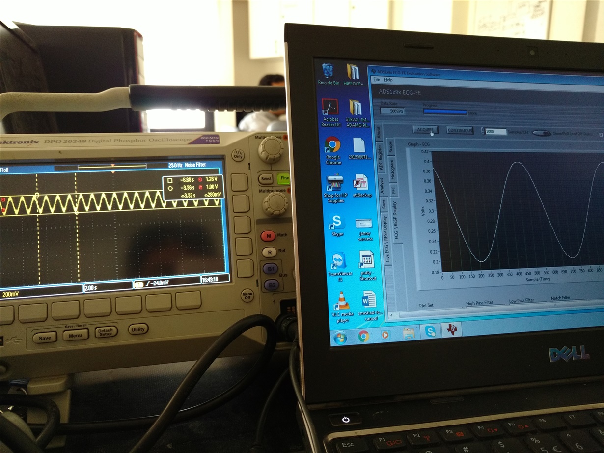
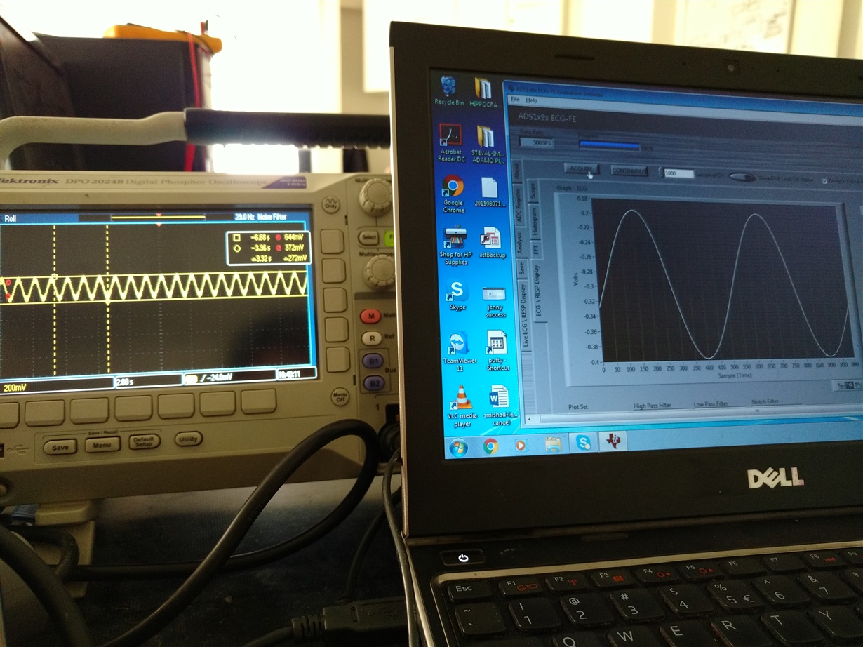
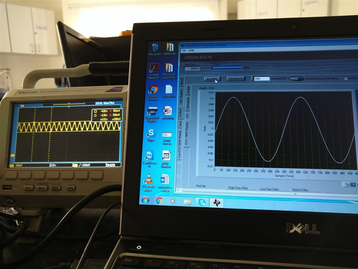
I have done the configurations of register & i can faithfully see the applied input,on PGA (output after gain of PGA)pins on the EVM software as well as on the DSO.  
  • Hello Rushit,

    There is a typical +/-100uV differential offset voltage for each channel on the ADS1292. A differential offset voltage at the inputs of each channel will be multiplied by the PGA gain and appear at the PGA output between the PGAxP and PGAxN pins. Is this what you are measuring? Please confirm that you are measuring differentially between the PGA output pins and give us the magnitude of the offset voltage and the PGA gain setting.

    The channel offset voltage can be calibrated using the OFFSETCAL command. Whenever you change the PGA gain, you should send this command. The device will internally short the inputs together and take several samples to calculate an offset calibration value for each channel.

    Best Regards,
  • I have set the PGA gain to 1,so there will be no amplified offset & yes i am measuring between PGA2P & N.

    For your reference please find attached the images which have EVM SW(shows the output original signal applied) & DSO measuring the diff. voltage across PGA2P & 2N.

    Please let me know why there is offset @ o/p of PGA,is there a setting for it,how to do it.

    Secondly : I am making the same arrangement in my board but cannot get an offset on PGA as i am getting over here ,so as a result my board clips the -ve side of signal (till -300mv),where as the EVM does measure it faithfully.Both have the single supply same reg setting.

  • Hello Rushit,

    Thanks for the clarification.

    The channel offset specification includes the offset contributions of the PGA and the ADC modulator. It is possible that the PGA and modulator offsets are different and in some cases, they may "offset" each other. :)

    What are the applied input signals for each image? Please provide the intended differential offset as well as the peak-to-peak amplitude.

    Remember that you should be measuring differentially. The best approach would be to use two probes, each with its ground clip tied to the system ground, and use the scope MATH function to measure the differential PGA output.

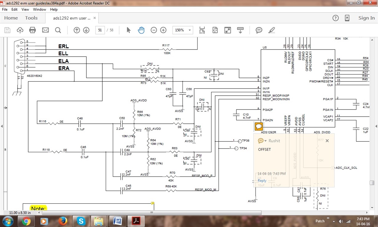
    With a single supply (0V = AVSS), you should not be driving either input pin with a negative voltage. If you exceed 300mV beyond the supply rails, you risk damaging the device. So, perhaps on the EVM, you are getting lucky in a sense and the inputs are not quite clipping yet. The plot below shows that one of the inputs will reach -200mV when a -300mV offset is given to the channel input.

    Regards,