This thread has been locked.

If you have a related question, please click the "Ask a related question" button in the top right corner. The newly created question will be automatically linked to this question.

ADC34J44: SYNC input

Other Parts Discussed in Thread: ADC34J44, CDCLVP1102

Hi all,
I would like to confirm the specification of SYNC pin of ADC34J44.
According to the datasheet, the VIH is 1.3V and VIL is 0.5V.
And it seems to be a single end level specification.
However the SYNC input is the differential.
How do I understand this specification?
Is the voltage from o,5V to1.3V the differential input voltage?

If yes,
when I want to use SYNC input as 1.8V CMOS single end,
is it possible following solution?

SYNCM~ is connected to 0.9V as Vcm
SYNCP~ is connected to 1.8V LVCMOS output.

If no, could you please tell me the single input method?
When I looked for the interface conversion IC from 1.8V LVCMOS to 1.8V LVPECL,
I could not find it at TI WEB site.
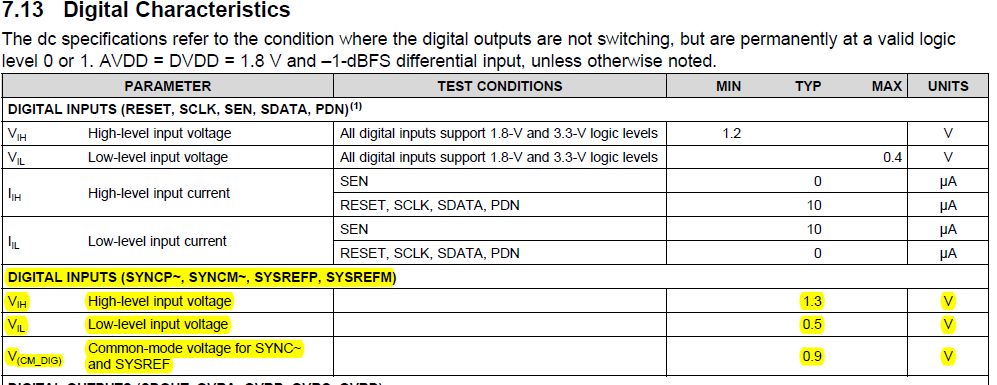

Regards,
Toshi

  • Hi Toshi,

    The SYNC input spec needs to be updated to have a more meaningful spec for input high and low. It is currently spec'd as a single ended level and should be spec differential. The typical specification for SYNC and SYSREF should be common mode of 0.9V with a +/-400mV swing. The differential voltage should be +400mV for a high and -400mV for a logic low.

    We have used LVDS signaling and it works fine. . You can use any of our LVDS or LVPECL buffers such as CDCLVP1102 or others in that family to buffer LVCMOS to LVDS/LVPECL.

    Ken.
  • Hi Ken-san,
    Thanks for your reply.

    I have some additional questions.

    1. Is there the minimum value of Vid (differential input voltage) of SYNC pins because the LVDS Vod is 350mV(typ)?

    2. I would like to confirm whether below my idea is ok or not.

    SYNCM~ is connected to 0.9V as Vcm
    SYNCP~ is connected to 1.8V LVCMOS output.

    3. CDCLVP1102 output is LVPECL and the nominal output common voltage is 2V.
    When using this IC, what is the recommended termination value for connecting to ADC34J44?

    Best regards,
    Toshi

  • Hi Toshi-san,

    1. There is no min or max spec on this differential swing at this point.  We will gather data and put that into the next data sheet release.  The input circuits will look for some differential voltage to switch either logic low or logic high.  I do not anticipate any issues with 350mVpp differential swing.

    2. We have not used a single ended signal into the SYNCP/M pins, however I believe that this will work.

    3. The CDCLVP output levels are dependent on the VCC.  You can also look for LVCMOS to LVDS translators in the same family of products.  Although we have not used any translators with this device specifically.

    Ken,