This thread has been locked.

If you have a related question, please click the "Ask a related question" button in the top right corner. The newly created question will be automatically linked to this question.

ADS7886 conversion data after powerup and restart

Other Parts Discussed in Thread: ADS7886

Hi

Our customer is evaluating this device.

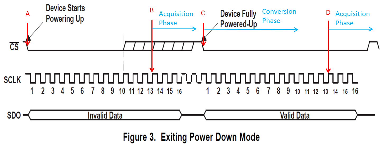
They have a question about conversion data after powerup and restart.

On the datasheet it is defined as the following spec,

I do not understand what this means?

Does it mean 1 conversion data? 

Regards,

Koji Hamamoto

  • Dear Hamamoto san,

    Yes, it means one invalid conversion data. One entire SAR ADC conversion needs two phases:  Acquisition phase and Conversion phase. One valid data can be retrieved if the SAR ADC's internal sampling capacitor has been fully charged during Acquisition phase before entering Conversion phase. Regarding to the timing as below, the first /CS low signal for more than 10 SCLK falling edges will bring the ADC out of power down mode and the device will be powered up from A point, the first Acquisition phase will start on the first rising edge of SCLK after the 13th falling edge (B point) and will charge the ADC's internal sampling capacitor,  then the falling edge of the following /CS signal (C point) will initiate the Conversion process and the valid data in MSB first format will be clocked out starting from the 4th falling edge of this second cycle. The next (second) Acquisition phase will start on the first rising edge of SCLK after the 13th falling edge  of of the same second cycle (D point) and will charge the ADC's internal sampling capacitor for next conversion.

    I hope this is helpful for you. 

    Thanks and Regards

    Dale Li

  • Hi Dale-san

    Thank you very much for your reply.
    That was very helpful explanation for me.

    May I ask one more question?
    Is that possible to input to VIN and SCLK and CS before supplying VDD?

    Regards,
    Koji Hamamoto
  • Hi Hamamoto-san,

    From ADS7886's Absolute Maximum Ratings table also as below, it's not a problem for Digital input which is not limited to ADC's +VDD, but it will be a potential problem for analog input (Vin or +IN) because the rating range of Vin(or +IN) is between -0.3V and +VDD+0.3V, so the Vin should be available later than +VDD or at the same moment. For best practice, power up +VDD firstly.

    Please let me know if you have more questions, thanks.

    Regards

    Dale Li