This thread has been locked.

If you have a related question, please click the "Ask a related question" button in the top right corner. The newly created question will be automatically linked to this question.

FS/4 in AFE7225

Other Parts Discussed in Thread: AFE7225, AFE7222

Dear

End customer is reviewing and considering to use AFE7225.
Pls help to check below questions.

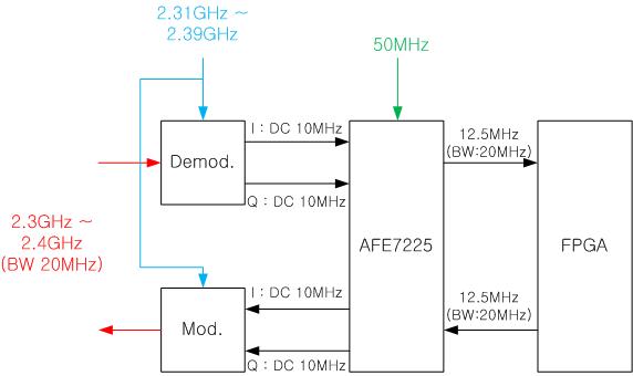
Q1. Their existing design is processing Fs/4 in FPGA. So if possible to use AFE7225 inner ‘FS/4’ as below block diagram?
Q2. Input-output data of IQ method(from AFE7225 to FPGA) is in order of ‘IQIQ’, is it right? Or “IIQQ”?
Q3. We have AFE7225EVM, TSW1400, but it`s hard to use it.
We need help about Config-file, Setting Guide for test below block diagram.
  • Henry,


    You can use coarse mixer for this. What is target sampling clock for ADC and DAC?

    Thanks,

    KW

  • sample rate is 50Mhz
    Fs is 2.3Ghz
  • Henry,

    AFE7225 has max 250Msps of DAC and 125Msps of ADC.
    AFE7222 has max 130Msps of DAC and 65Msps of ADC.
    AFE722x supports 1/2/4 of interpolation and 2 for decimation. Flexible clock scheme is provided with Internal clock divider (1/2/4) for ADC and DAC.

    If this customer follows 3GPP, suggested clocks are 245.76/122.88/61.44Msps respectively. As AFE722x has clock divider for ADC internally, 122.88Msps of clock can be used for ADC from 245.76Msps of external clock input for DAC. You are saying 50MHz of clock and this is not clear to me. And also, you mentioned 20MHz of signal bandwidth. Is this application repeater for LTE or something?

    You mentioned Fs is 2.3GHz. In general, Fs is referred to sampling clock. It looks like you are saying RF frequency for external modulator/demodulator stage and this is not related to AFE722x configuration.

    Thanks,
    KW