Hi,
We are currently testing the TSW54J60 EVB (paired with TSW14J56) and have a couple of questions.
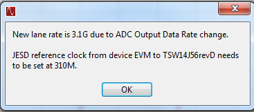
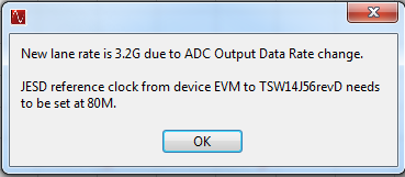
First, I have a lack of knowledge in the JESD204B protocol. In HSDC Pro, if you enter a sampling frequency of 500 MHz for the ADC you will need a JESD core clock of 125 MHz. This comes from the 2 lanes we use per ADC (LMFS4211 configuration) and we have to divide the JESD data rate /40 (5Gsps becomes 125Msps). Now there is an hard coded trick in the ADC configuration that makes it so when you go under 3.125Gsps data rate (78.125MHz core clock), the software will instead ask for the same core clock as the sampling clock (300 MHz sampling = 300 MHz core clock).
The exact line that does this in the ADC firmware config file must be the following (in ADS54J60_LMF4211.ini) :
MIF Config= 0.611G to 0.7G:RX:RX_PMA_x5,0.7G to 3.125G:RX:RX_PMA_x10,3.125G to 10.25G:RX:RX_PMA_x40
My understanding is this is a way to bypass the minimum FPGA transceiver frequency (which may be around 80 MHz). If this is true, then how come is the behaviour of having a 320 MHz data rate be the same as having a 80 MHz data rate in JESD204B?
My second question is about the setup of the LMK04828 which generates the clocks required on the EVB.
Using an R divider for OSCin of 1024 and an N divider for feedback of 12288 should do the same as using an R of 2048 and N of 24576. (same ratio)
For some reason, the PLL locks correctly with an R of 1024 but will not lock at 2048 nor 4096. I thought there could be a minimum phase detector frequency, but there is only a max of 155 MHz.
We'd like to use a large oscillator divider ratio to get more resolution in changing frequencies.
Any thoughts on this ?
Thank you,
Philippe