This thread has been locked.

If you have a related question, please click the "Ask a related question" button in the top right corner. The newly created question will be automatically linked to this question.

ADC32RF45EVM HSDC Capture Error

Other Parts Discussed in Thread: ADC32RF45EVM, ADC32RF45, LMK04828

Hello,

I have the ADC32RF45EVM and the TSW14J56 rev B board I am looking to get set up to start the evaluation process of this ADC.

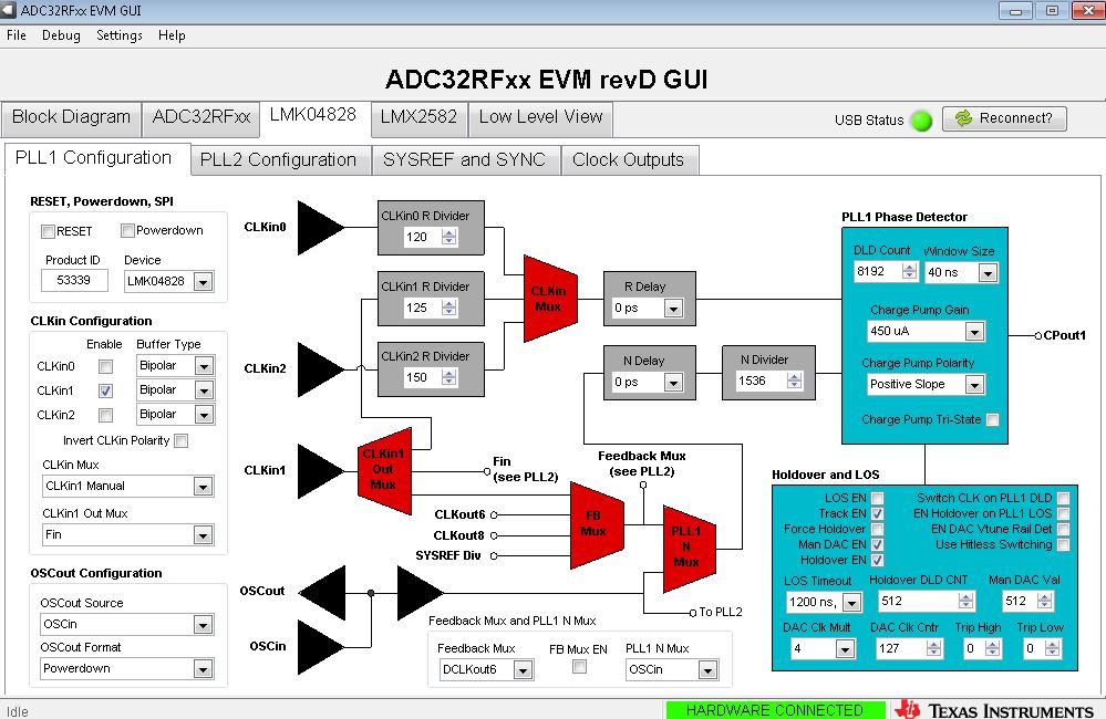
I am going through the Quick-Start Procedure ADC32RF45 Bypass LMFS82820 Mode procedure outlined in the user manual (pg. 6) for the ADC32RF45EVM.

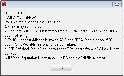
I have set-up the test equipment accordingly, and have allocated the appropriate ini files in the correct path in the HSDC install location for the rev B capture board. In HSDC I am getting no data on the FFT plot. Below is an image of the dialog box I am getting when I try to capture data.

My debug leds (D8:D1) on the capture board are as follows:

D8-Solid

D7-Extinguished 

D6-Extinguished 

D5-Solid

D4-Blinking

D3-Solid

D2-Blinking

D1-Extinguished

From the dialog box suggested possible reasons for time out error my clock from the ADC evm is not received by the capture board.

My  filtered signal generator is set for +15dBm @ 1.9GHz and is hooked up (t'ed off) to J5 and J7. The jumper JP3 is set for an ext. clock.

Thanks!


  • Hi,

    I would like to see screenshots of the HSDCPro and the SPI GUI setup before I could begin to guess.   Particularly HSDCPro, as I would like to see the revision of the GUI, the firmware name in the lower right corner, and pretty much everything else on that screen so I can see your conditions.

    For the SPI GUI for the EVM, I'd want to see that on the LMK04828 PLL1 tab that the SPI read back the device ID and type to know that the SPI is working.  And on the PLL2 tab the VCO selection would be 'external' and on the SYSREF tab the sysref divider would be 640.  On the ADC tab, I like to pick a random control and click it to make sure the SPI interface is working.  like pick the channel A scramble enable and see that it stays clicked.  then click it off again.   if I try to click on a control and it won't *stay* clicked but just falls back to off right away, then I know the ADC SPI is not working.  Reasons why the ADC SPI might not be working would be not having the sample clock *and* sysref present to the ADC when loading the ADC config file.  That is why the order of configuring the EVM is important - reset the LMK, configure the LMK, reset the ADC by way of the pushbutton switch, and then configure the ADC.  And then press the 'read all' button and go check that the ADC configuration on the ADC tab looks correct  and behaves correctly.

    Regards,

    Richard P.

  • Please take a look at the screenshots above.

    The VCO is set to external.

    The sysref divder is set to 640.

    It appears SPI is working as I picked a random control and it stayed enabled/clicked.
  • Hi,

    Thanks.  yes, it does look like the clocking and sysref is getting to the ADC as it looks like the ADC SPI interface is working.  But there remains one issue.  Your first post said the clocking was at 1.9GHz which I guess was a typo as the HSDCPro is set up for 2.94912Gsps as described in the user guide.  But the FPGA on the TSW14J56 revB is not capable of that rate.    If it were 1.9Gsps as mentioned in the first post then it would have been fine.   At 2.94912Gsps the line rate on the JESD204b in the LMFS82820 mode is right around 12 Gbps.     The FPGA in the revB capture card is good for around 10Gbps or so in its current state.    That means that at around 2.7Gsps into the ADC we begin to see bit errors popping up in the captured data in the FPGA and closer to 3Gsps it might not initialize a link at all.  

    For debug purposes, could you drop the sample clock down to around 2.5GHz and see that the setup if functional otherwise?  Then if so, then I think we need to get you on to the revD version of the TSW14J56.   In the revD capture card, there were improvements in the speed of the memory where the data is stored during capture and the speed of the bus between the FPGA and the memory, but the bigger thing was that the adaptive equalizer front end of the FPGA JESD204b link was enabled to allow for a higher data rate on the serial lanes. 

    Regards,

    Richard P.