


Hi,
I am working with ADS1292 using MSP430F5659 controller SPI. I have done the firmware referring the ADS1292ECG-FE firmware coding.
I am able to read and write the register, but i am not able to read the ADC value from channel 2 when i vary the input, it give constant value always.
What could be the problem here.
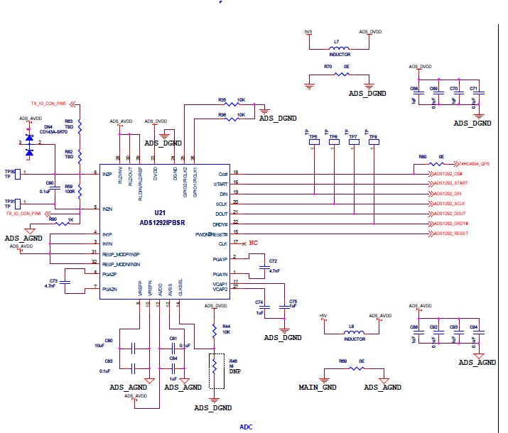
I have selected internal CLK and internal Reference voltage. Please refer the attached h/w interface diagram.
ADC is running @ 500 SPS, SPi clock is 1M for initialization phase as well as Data read
My initialization routine will follows here which is similar to ADS1292ECG-FE firmware init.
Ex_ADC_Init()

{

ADS1x9x_PowerOn_Init();

//Filter_Option = 3; // Default filter option is 40Hz LowPass
Start_Read_Data_Continuous(); //RDATAC command
for ( i =0; i < 10000; i++);
for ( i =0; i < 10000; i++);
for ( i =0; i < 10000; i++);

ADS1x9x_Disable_Start();
ADS1x9x_Enable_Start();

for ( i =0; i < 10000; i++);
for ( i =0; i < 10000; i++);
for ( i =0; i < 10000; i++);

Set_Device_out_bytes();

}

ADS1x9x_PowerOn_Init()

{

Init_ADS1x9x_Resource();
ADS1x9x_Reset();
for (j = 0; j < DELAY_COUNT; j++)
{
for ( Init_i =0; Init_i < 20000; Init_i++);
for ( Init_i =0; Init_i < 20000; Init_i++);
for ( Init_i =0; Init_i < 20000; Init_i++);
}
Init_ADS1x9x_DRDY_Interrupt();
//ADS1x9x_Clock_Select(1); // Set internal clock
for ( Init_i =0; Init_i < 20000; Init_i++);
for ( Init_i =0; Init_i < 20000; Init_i++);
for ( Init_i =0; Init_i < 20000; Init_i++);
ADS1x9x_Disable_Start();
ADS1x9x_Enable_Start();

Hard_Stop_ADS1x9x();

Start_Data_Conv_Command();

Soft_Stop_ADS1x9x();

for (j = 0; j < DELAY_COUNT; j++)
{
for ( Init_i =0; Init_i < 20000; Init_i++);
}
Stop_Read_Data_Continuous(); // SDATAC command
for (j = 0; j < DELAY_COUNT; j++)
{
for ( Init_i =0; Init_i < 35000; Init_i++);
}
for (j = 0; j < DELAY_COUNT; j++)
{
for ( Init_i =0; Init_i < 35000; Init_i++);
}
ADS1x9x_Read_All_Regs(ADS1x9xRegVal);
ADS1x9x_Default_Reg_Init();
ADS1x9x_Read_All_Regs(ADS1x9xRegVal);

}
I dont whether i am doing any wrong initialization or is there any h/w issue.
SPI init routine is shown below
void Set_UCB0_SPI(void)
{

uint8_t returnValue=0;

P2SEL |= BIT1+BIT2+BIT3; // Set SPI peripheral bits
P2DIR |= BIT1+BIT3; // Clock and DOUT as output MOSI & CLK
P2DIR &= ~BIT2; // Din as input MISO
UCB0CTL1 |= UCSWRST; // Enable SW reset
UCB0CTL0 |= UCMSB+UCMST+UCSYNC; //[b0] 1 - Synchronous mode
//[b2-1] 00- 3-pin SPI
//[b3] 1 - Master mode
//[b4] 0 - 8-bit data
//[b5] 1 - MSB first
//[b6] 0 - Clock polarity low.
//[b7] 1 - Clock phase - Data is captured on the first UCLK edge and changed on the following edge.

UCB0CTL1 |= UCSSEL__ACLK; // ACLK
UCB0BR0 = 24; // 1 MHz
UCB0BR1 = 0; //
UCB0CTL1 &= ~UCSWRST; // Clear SW reset, resume operation

}
DRDY interrupt init routine
void Init_ADS1x9x_DRDY_Interrupt (void)
{

P3DIR &= ~0x02;

P3REN |= BIT1; // Enable P3.1 internal resistance
P3OUT |= BIT1; // Set P3.1 as pull-Up resistance
P3IES |= BIT1; // P3.1 Lo/Hi edge
P3IFG &= ~BIT1; // P3.1 IFG cleared
P3IE &= ~BIT1; // P3.1 interrupt disabled

}
start ADC function is called for the continuous read data command and data ADC start conversion
Start_Ex_ADC()

{

ADS1x9x_Disable_Start(); // Disable START (SET START to high)

Set_ADS1x9x_Chip_Enable(); // CS = 0
__delay_cycles(300);
Clear_ADS1x9x_Chip_Enable(); // CS = 1

UCB0CTL1 |= UCSWRST; // Enable SW reset
UCB0CTL0 |= UCMSB+UCMST+UCSYNC; //[b0] 1 - Synchronous mode
//[b2-1] 00- 3-pin SPI
//[b3] 1 - Master mode
//[b4] 0 - 8-bit data
//[b5] 1 - MSB first
//[b6] 0 - Clock polarity low.
//[b7] 1 - Clock phase - Data is captured on the first UCLK edge and changed on the following edge.

UCB0CTL1 |= UCSSEL__ACLK; // ACLK
UCB0BR0 = 2; // 12 MHz
UCB0BR1 = 0; //
UCB0CTL1 &= ~UCSWRST; // Clear SW reset, resume operation

Set_ADS1x9x_Chip_Enable(); // CS =0
__delay_cycles(300);
Start_Read_Data_Continuous(); //RDATAC command
__delay_cycles(300);
ECG_Recoder_state.state = ACQUIRE_DATA_STATE; // state = ACQUIRE_DATA_STATE
ECG_Data_rdy = 0;
Enable_ADS1x9x_DRDY_Interrupt(); // Enable DRDY interrupt
ADS1x9x_Enable_Start(); // Enable START (SET START to high)


}
On interrupt i.e. DRDY port interrupt SPI count is made zero and data is gathered . Both interrupts are given below
// DRDY port pin interrupt
void Port3_int(void)
{


if ( P3IFG &= BIT1)
{
P3IFG &= ~BIT1; // Clear P3.1 IFG i.e Data RDY interrupt status
SPI_Rx_Count = UCB0RXBUF; // Dummy Read
SPI_Rx_Count=0;

UCB0TXBUF = 0;
UCB0IE |= UCRXIE; // Enable USCI_B0 RX interrupt
//Enable Receive interrupt
USCI_B_SPI_clearInterrupt(USCI_B0_BASE, USCI_B_SPI_RECEIVE_INTERRUPT);
USCI_B_SPI_enableInterrupt(USCI_B0_BASE, USCI_B_SPI_RECEIVE_INTERRUPT);

//Disable_ADS1x9x_DRDY_Interrupt(); // Enable DRDY interrupt
}

}


void SPI_B0(void)
{


switch(__even_in_range(UCB0IV,4))
{
case 0:break; // Vector 0 - no interrupt
case 2: // Vector 2 - RXIFG

while(!USCI_B_SPI_getInterruptStatus(USCI_B0_BASE,
USCI_B_SPI_TRANSMIT_INTERRUPT))
{
;
}

receiveData = USCI_B_SPI_receiveData(USCI_B0_BASE);
SPI_Rx_buf[SPI_Rx_Count] = receiveData;
SPI_Rx_Count++;
if ( SPI_Rx_Count == SPI_Rx_exp_Count)
{


//UCB0IE &= ~UCRXIE; // Disable USCI_B0 RX interrupt
USCI_B_SPI_clearInterrupt(USCI_B0_BASE, USCI_B_SPI_RECEIVE_INTERRUPT);
//ADS1x9x_Parse_data_packet();
ADS1292x_Parse_data_packet();


}
else//data
{


transmitData=0;

//Send next value
USCI_B_SPI_transmitData(USCI_B0_BASE,
transmitData);


}
//Delay between transmissions for slave to process information
__delay_cycles(40);
break;
case 4:break; // Vector 4 - TXIFG

default: break;
}

}
Please let me know any thing i am missing , i need urgent help
Any suggestions are welcome.
Nitesh


