This thread has been locked.

If you have a related question, please click the "Ask a related question" button in the top right corner. The newly created question will be automatically linked to this question.

Reading RREG ADS1298

Other Parts Discussed in Thread: ADS1298

Hi all,

I am trying to read the ADS1298 RREG register using OPCODE and I don't get any feedback from the MISO port.

for example lets say I write :

// 7) Configures all channels as input-shorted
eeg_spi_buff[0] = 0x45;
eeg_spi_buff[1] = 0x07;
eeg_spi_buff[2] = 0x01;
SpiMasterTransfer(eeg_spi_buff, 3, 0, 0);

And immediately after I want to read if the configuration has been upload, so I do this:

//Read  8 registers at address 0x05 
eeg_spi_buff[0] = 0x25;
eeg_spi_buff[1] = 0x07;
SpiMasterTransfer(eeg_spi_buff, 2, 0, 0);

This is how I initialize the ADC:

// SEQUENCE OF COMMANDS:
// 1) Send RESET Pulse
// 2) Send SDATAC command
// 3) Configure Reference Buffer
// 4) Configure Clock Setting
// 5) Set input-shorted

// 6) Read RREG

// 8) Send START command
// 9) Send RDATAC command to enable continuous data capture
// 10) Wait until Data is received and Read Captured data
// 11) Send SDATAC command

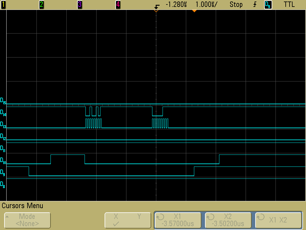
Well, if I enter RDATAC to get the conversions i can see (using an oscilloscope) data in the MISO port.

But if I do only until step 6, there's no way I see the configuration through the MISO.

Any clue, with what is happening? Do I have to do any thing special, besides stopping the RDATAC to read RREG?

Thanks

  • Hey Conrad,

    Can you capture the RREG transaction with an oscilloscope for me to review?

    Brian
  • Hey Brian,

    Yes sure!

    The following screenshot has been taken after doing:

    1) RESET

    2)SDATAC

    3) WREG CONFIG3 with value 0xCC

    4) WREG CONFIG1 with value 0xC6

    5) WREG CHnSET for all 8 REG (NREG = 8-1) with value 0x01 for 0x07 Registers.

    6) Perform a RREG 0x25 for 0x07 registers.

    In the screenshot the labels are:

    D9 Debbug pin which I set low at the beginning of step 6) and set high after it finishes.

    D10 ADC CS

    D13 SCKL (SPI CLOCK)

    D14 MOSI

    D15 MISO

    What it should appear after the two bytes sent through SPI in the MOSI signal is that the information of CHnSET should be in the MISO signal after the command is send  and before the D9 sets high.

  • Conrad,

    You will need to extend SCLKs to shift out the register data. SCLK runs the interface state machine so MISO will not output data without SCLK.

    Brian