This thread has been locked.

If you have a related question, please click the "Ask a related question" button in the top right corner. The newly created question will be automatically linked to this question.

AFE7225 set of values

Other Parts Discussed in Thread: AFE7225, CDCE72010

Dears.

Can I get config file for this operating case?

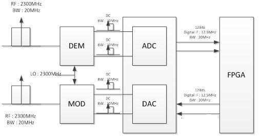
-       AFE7225 operating CLK is 61.44MHz

-       RF 2300MHz is changed DC I and Q through demodulator

-       Through demodulator in internal ADC, the signal is changed Digital IF 12.5MHz BW : 20MHz

-       ADC OUT CLK 50MHz and 12Bits Digital IF 12.5MHz, BW 20MHz signal transmit 1 time per a CLK

-       FPGA read the data to work to ADC OUT CLK

-       FPGA transmit DAC IN CLK and 12Bits Digital IF 12.5MHz, BW 20MHz signal 1 time per a CLK

-       DAC make to change analog DC I and Q through modulator

-       DC I and Q signal in modulator make RF signal 

It is difficult to test with AFE7225EVM

The CDCE72010 does not output0, output4 from the AFE7225EVM.

When the CLK input J10 port, CLK is reversed in signal generator. 

  • Hi, Henry


    What is the clock divider ratio for ADC clock? There is clock divider for ADC. If DAC clock is 245.76MHz, ADC clock is 122.88MHz by using clock divider '2'.

    ADC clock and DAC clock can be set different by using clock divider. If sampling clock is 61.44MHz with coarse mixing, 20MHz of IBW can be located at 15.36MHz by using coarse mixer. Harmonics of carrier will be located at every 61.44MHz. I don't think this is a good system architecture. What is the interpolation ratio for this system?

    Thanks,

    KW