This thread has been locked.

If you have a related question, please click the "Ask a related question" button in the top right corner. The newly created question will be automatically linked to this question.

Simple schematic for EMG using ADS1298

Other Parts Discussed in Thread: ADS1298, ADS1299

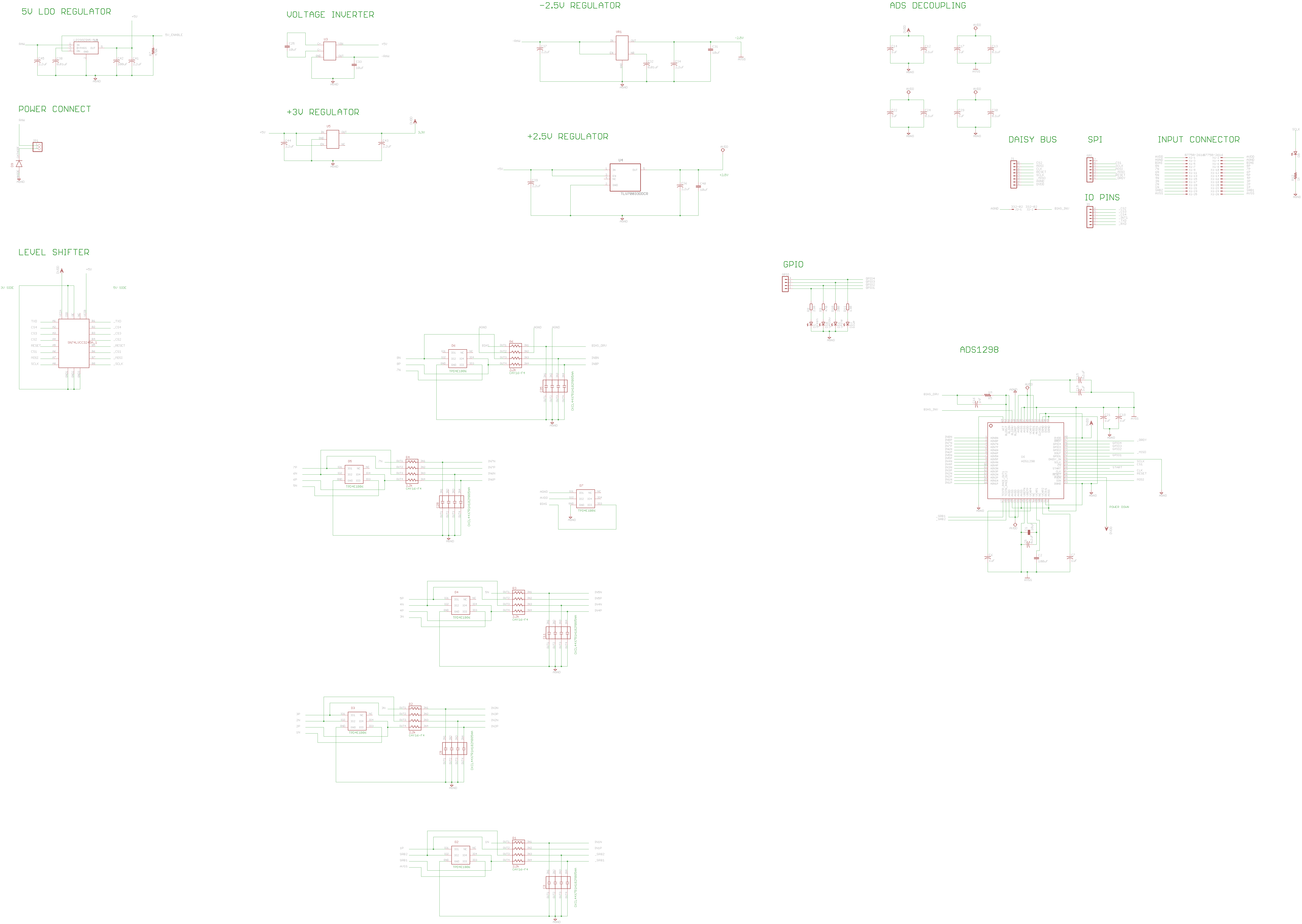
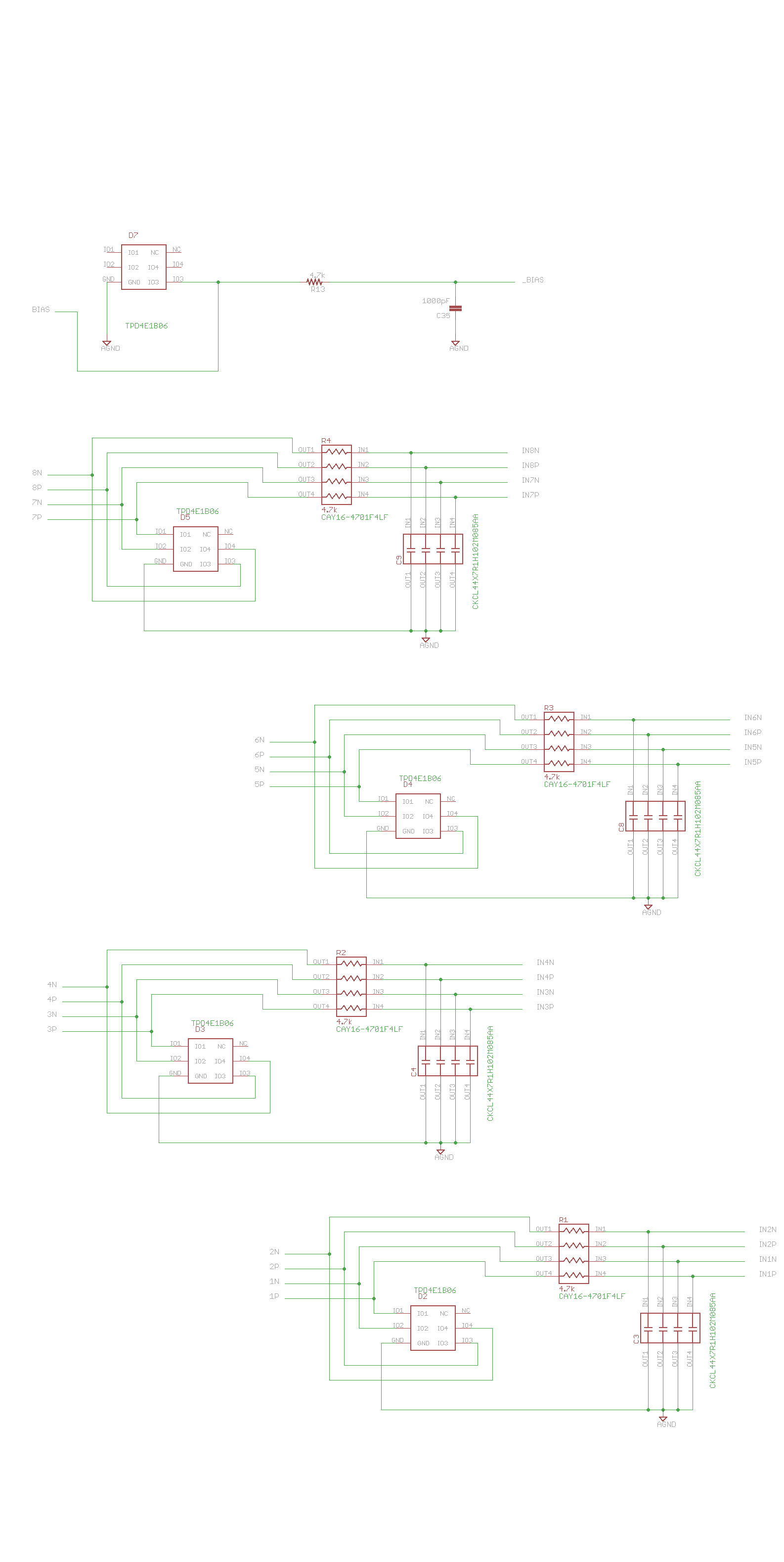
Hi everyone, I'm trying to draw simple schematic for EMG based on ADS1298. I want to connect it via SPI to STM32F4 discovery. So, can I ask you to check my schematic and help me to understand how to connect common reference electrode (I'm planning to use all 8 channels). As far as I know we use only one common electrode for this chip. How it will affect to my other channel if I place this electrode on elbow for example (other electrodes are placed on biceps, triceps, trapezius, etc).

And how can I connect RLDs pins for measuring EMG. Also, according datasheet I can use 2 chips and get 16 channels. It could be using DAISY_CHAIN or

Slave -> Master <- Slave connection (SPI). If I'd like to use daisy chain, how can I draw my schematic for this purpose.

I have a level shifter to use it with Arduino (probably), cause it has 5V pins. As I know stm32 SPI works well without shifter

My schematic

  • Hello Ivan,

    Unfortunately I am unfamiliar with the clinical aspects of EMG (like electrode placement, etc.), but I can certainly advise you as to how to properly use the ADS1298.

    It appears that you've adapted this schematic from another that used the ADS1299 since you still have "SRB" connections and a "Bias" electrode. The ADS1298, however, does not have "SRB" capabilities so those connections should be removed. If you want to collect data with respect to a single reference electrode, that electrode will have to be routed to the INxN pins for each channel.

    The RLD can be configured like it is shown in Figure 43 of the ADS1298 datasheet. The feedback loop between RLDOUT and RLDINV must be closed if you expect the common-mode rejecting features to work properly.

    For details on multi-device configurations, refer to section 9.4.2 of the ADS1298 datasheet which begins on page 56.

    An error I noticed: do not connect the WCT pin to ground. This can create a short circuit.

    Regards,
    Brian
  • Thanks for your reply. The bias electrode is used only with ads1299, isn't it? 

    I found several schematics there are RLD is routed to both pins INP and INN, you mentioned to connect it to INN. I can't realise how to use it? And if I connect RLD to channel, should I use a resistor in my connection?

    One of those schematics processors.wiki.ti.com/.../SCHEMATIC-ADS1298_Test_Circuit.pdf

    And WCT, most of found schematics have this pin connected to AGND via capacitor, is it correct?

    And can I use ads1298 for emg and ecg purposes. I mean 7 channels are measuring emg and the 8th channel is measuring ecg for heart rate tracking

  • Hello Ivan,

    Yes that is true. But the bias on the ADS1299 and the RLD on the ADS1298 function in the same way - bias the patient so some known voltage.

    I'm not sure what you mean. Why are you trying to connect the RLD to both channel inputs? That schematic does not show the RLD connected to channel inputs.

    Yes the WCT is usually shunted to ground via a capacitor. Your schematic shows it directly connected to ground, which is a short circuit.

    The ADS1298 should be ok for EMG as long as the signals you wish to measure are larger than the input referred noise specifications of the ADS1298. You can find the noise statistics in the tables beginning on page 22 in the datasheet.

    Regards,
    Brian Pisani
  • Indeed, it seems to me I was wrong with RLD example schematics, but I saw some "working" schematics where inputs are routed to RLD. Nevertheless, according to datasheet, this chip has 2 modes of RLD (external and internal). Does this mean that I can measure EMG without RLD electrode (configure it in other way). If I understood correctly, if I set RLD as internal mode my common reference will be initialised inside the chip. And I will have only 8 pairs of input electrodes instead of 8 pairs + 1 electrode. Am I right?

    And I 'm confusing about power supply. Page 76 Figure 74 shows +- 1.5V for bipolar analog supply and + 1.8V for DVDD. My schematic, which I adapted from ADS1299 has +-2.5V and +3.3V for DVDD. Is it okay for ADS1298 or I must change it according to datasheet?

    And one more question, I guess I a little bit confused, can I use schematic for ECG to measure EMG without changes or I must change for this purpose? I mean are the signals the same or not (I watched a couple of videos where guys measure EMG with ADS1298ECG-FE)

    And big thanks for your reply, I think it 's becoming more understandable for me now.
  • Hey Ivan,

    You will need some way of biasing the patient's voltage. Even if you were to use the RLD output as a reference on the board for measuring the channels, there is nothing keeping the patient electrode voltages from swinging well outside the range of the ADC. I would recommend using a separate RL electrode or some other reference electrode with an actively regulated voltage that is connected to the patient.

    The +/-2.5V analog supply and +3.3V digital supply are a valid configuration.

    The only difference that I am aware of between EMG and ECG is the magnitude of the signals. As long as the intended signal magnitude is larger than the noise level on the ADS1298, then I do not believe any special considerations must be made.

    Brian
  • Brian, thank you for your reply!

    What is better to use 1 low-pass filter or 2? My schematic uses 1 low-pass filter, is it enough to read more quality signal without noises? And what are the values of resistor and capacitor better to use to decrease the noise?

    So, and my question about RLD, if I wanna use my external RLD electrode, I have to connect RLDOUT to RLD electrode (with low-pass filter and ESD protection such as channel's pins), I connect RLDIN to RLDINV via 1M resistor and 1.5nF capacitor, which are connected in parallel way, RLDREF to AGND and WCT via capacitor to AGND too. Am I right?
  • Ivan,

    Using a second order RC low-pass filter will likely provide better anti-aliasing, but it may not be required. The relevant formula then is fc = 1/(2*pi*R*C). The resistor R can double as your patient protection resistor, so you can pick that value first. Then I recommend you pick C such that fc is somewhere around 32 kHz. The ADS1298 is a delta-sigma ADC, so sampling happens significantly faster than the output data rate.

    That is a valid RLD connection scheme!

    Regards,
    Brian Pisani
  • I found that passband is recommended for EMG should be 65-70 Hz for LPF and HPF be 150-180 Hz. You mentioned 32kHz. Can't understand why is so different?

    According to 2 stage LPF, many of schematics use it.

  • Hey Ivan,

    The ADS1298 is a delta-sigma ADC which is a type of ADC where data is sampled at a high frequency, digitally filtered, downsampled, and output at a lower data rate. For example, on the ADS1298 when the device is configured in high-resolution mode, the delta-sigma modulator runs at 512 kHz. The digital filter behavior is specified starting on page 49 of the datasheet. Essentially the band will be limited based on the data rate you chose and the only aliasing you need to worry about is around 512 kHz since that is where the digital filter response repeats. Thus a 32 kHz cutoff for your anti-aliasing filter should be sufficient.

    Further, passive components tend to have relatively large tolerances compared to matched components on integrated circuits. This means that putting two RC anti-aliasing filters on both the positive and negative inputs of a channel with a low cutoff frequency will produce pretty bad CMRR. CMRR is an extremely important specification for medical applications since electrodes and bodies tend to act like big antennae picking up power line interference from overhead fluorescent lights. By placing the cutoff frequency of the anti-aliasing filter out past the bandwidth of interest and relying on the digital filter for reducing noise, you will improve CMRR in a huge way.

    Regards,
    Brian Pisani
  • Thanks for you explanations, so I understood that I have to get 32kHz of frequency using 2 RC filters.

    I use the formula 1/2*PI*sqrt(R1*C1*R2*C2), am I right? Or I can use 1 RC to get 32 kHz.

    If 2 RC filters give me 32 kHz and 1 RC gives me 32 kHz, will have it the same effect?

    Could you recommend me a couple of RC for using with this electrodes (positive and negative), cause I was trying to calculate fc of founded schematics to match them and I was getting the different variations:

    1. R1=22k C1=47pF R2=10k C2=47pF fc =  228kHz for 2 stage low-pass filter

    2. R=10k C=47pF fc=33.8 kHz

  • Hey Ivan,

    Single and double pole RC filters do not have the same transfer function. The formula I gave for fc only applies for a single pole RC filter. A single RC filter should be sufficient for this application. Your option 2 will probably achieve the purpose.

    Brian
  • Hi Brian, could you tell me, how can I connect RLD in daisy chain mode. Figure 45 of datasheet says that device1 has RLDINV connected to RLDOUT via resistor and capacitor, device n has no connection for RLDOUT and RLDINV connected to common RLD channel. Do I need to use jumper to select mode or all my devices can use resistor and capacitor to make a connection between RLDOUT and RLDINV and have a pin to connect them all together?
  • Hey Ivan,

    The purpose to having the all the RLDINV pins connect to a single RLD amplifier is to use only one amplifier to take common-mode feedback from all the different devices. If all RLDOUT pins were connected together, that would create a short circuit condition.

    You will likely need some form of logic to establish a difference between the single device and multiple device modes (whether it be by jumper, or by simply not populating the R and C during assembly of boards that will be in the "device 2-n" category).

    Regards,
    Brian Pisani
  • Hey Brian, thanks for yr reply. I'm worrying hot to combine 2 modes in one circuit. In a single mode daisy pin should be connected to AGND, for this purpose I will use jumper.  I found your answer in other thread, you had recommended to use cascade mode instead of daisy chain

  • Hey Ivan,

    I do recommend a cascaded configuration since using the daisy_in pin is a little tricky. Do you have a question about how to do this?

    Brian
  • According to datasheet, it works like a simple master - slaves connections,  isnt it? I have one more question about schematic, do i need to connect to

    avdd those channels which are not used?

  • Hey Ivan,

    Yes essentially each device will have its own CS line which serves to select it for communication. They can be synchronized by sharing a clock and a START signal. It is not required to connect the unused channel inputs to AVDD but it is recommended to improve power consumption.

    Brian
  • If it's used to improve power consumption, I'll miss this connection via jumper, cause for dev board I'm not going to use battery, only power via usb. I'm also confusing about power regulation. I'm going to use stm32f4discovery as MCU (master). It has +5v and +3.3v pins. Logically I don't need the circuit for generating those volts on my ads1298 pcb. Am I right? I just need to make +2.5v and -2.5v, is it correct? In other words is it possible to use power pins from another dev board which generates +5v and +3.3v? I haven't checked data sheet of stm32, but I guess the power regulations are similar
  • Ivan,

    This device allows for a unipolar supply configuration. If it's easier, you can simply use those voltages you mentioned to power the ADS1299. The only other thing to take into account is the current capacity of those power supplies. Verify that it will be able to power the ADS1299.

    Otherwise if you require a bipolar supply configuration, you can generate that +/-2.5 V on your own.

    Regards,
    Brian Pisani
  • Hey Brian, I reconfigured my schematic, could you please check it for mistakes?

    Also, Figure 109 of datasheet recommends to use resistors on SPI lines to prevent reflection. Is it necessary to connect SPI of slave to master via those resistors, my main MCU SPI pins have 3.3V.

    And I decided to pass voltage regulation circuit, cause according to datasheet +3.3V should has around 250mA of current, but my MCU has up to 180 mA, so can I use my MCU's +5V as a RAW POWER?

  • Hey Ivan,

    The schematic looks fine.

    I wouldn't worry about digital communication reflections if the processor is reasonably close to the ADS1299.

    The ADS1299 will consume less than 10 mA when using a 5 V AVDD and 3.3 V DVDD. Either source should be sufficient to power the device. The logic level for communication should be equal to DVDD.

    Regards,
    Brian Pisani
  • The processor is too far (aprox. 10 cm) from ADS1298, they will be connected by wires, it is 2 different pcbs. My processor has 3.3V on SPI lines, I think it's enough and I don't need shifter, am I right? And what about the schematic, is it correct?
  • Ivan,

    As long as you are also using 3.3V for DVDD then you should be fine. The schematic looks good.

    Brian