This thread has been locked.

If you have a related question, please click the "Ask a related question" button in the top right corner. The newly created question will be automatically linked to this question.

High Resolution Decay Measurement

Other Parts Discussed in Thread: ADC12J4000EVM, TSW14J50EVM, LMH5401EVM, OPA659EVM, OPA659, LMH5401, ADC12J4000, TSW12J54EVM

Hello,

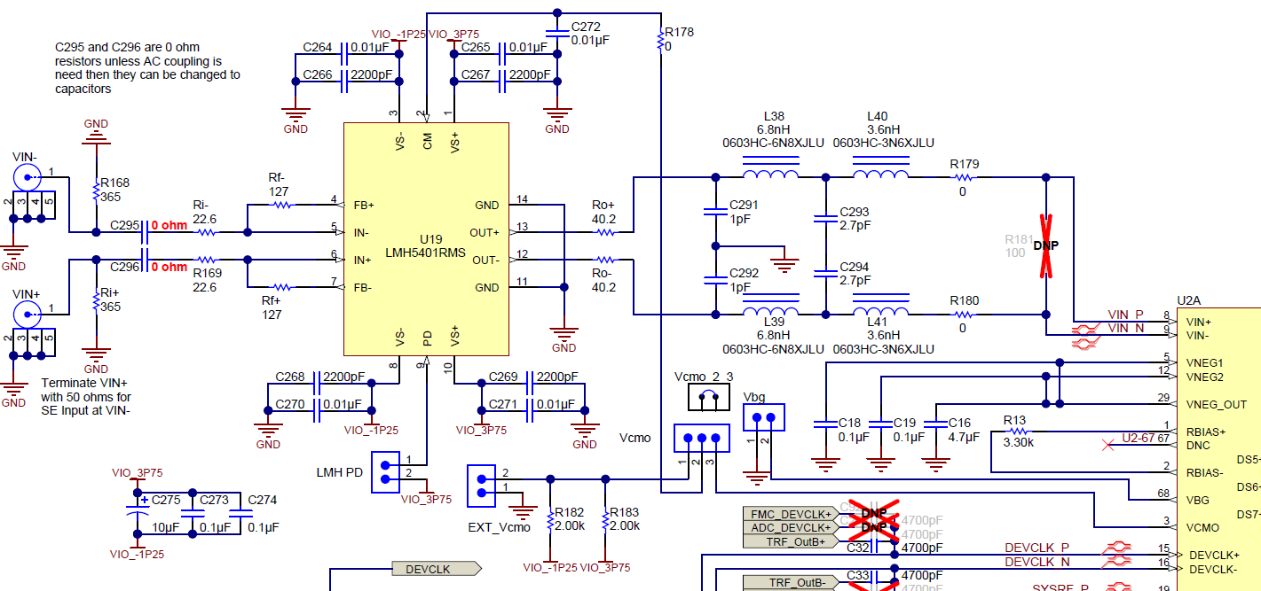
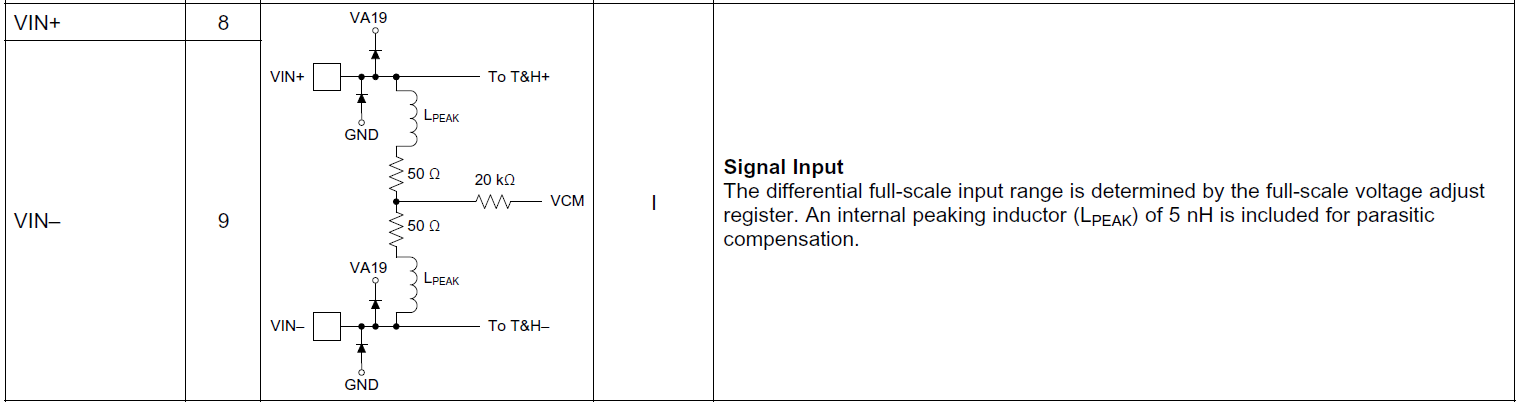
We are wanting to perform decay measurements of a signal that can range from 1.5V to 0V.  We are looking at the AD9625-2.0 evaluation board to measure the decay at greater than 1 GS/sec.  Since nobody in our group is too familiar with high speed data acquisition devices, can someone help with all the hardware needed to make a decay measurement with nanosecond resolution?  From what I've seen in the documentation, an FPGA is needed to read and store the data at that fast of a rate.  Then, a computer can read the data from the FPGA.  Is anything else needed?

Thank you in advance for your help.

  • Hi Alex

    Can you describe your intended measurements in more detail? Minimum and possible maximum sample rate, capture record length, etc?

    Most of these ADC evaluation tools store the data to on-board high speed memory, then the data is transferred to the computer at slower speed for display and analysis. At 1 Gs/s, how many samples do you need to store in a continuous record to meet the needs of your application?

    Depending on the depth you need there may be better tools I can recommend. The capture board associated with the AD9625-2.0 eval board has a memory size of only 256kB.

    Best regards,

    Jim B

  • Hi Jim,

    Thanks for the reply.  We need a minimum of 1 GS/s.  Higher than that is definitely good too.  We just want nanosecond resolution for the first hundred microseconds of the decay.  So, at 12 bits per sample, that means we would need a minimum storage of 1.2 MB for 100 microseconds of data capture time.  We would like to capture data for longer (about 10 seconds), but I understand that it might not be feasible to store so much data at once.

    Really, we would need less resolution as time went on.  After 100 microseconds, we wouldn't need nanosecond resolution.  Microsecond resolution would work just fine in that regime.  Then, after 100 milliseconds, 1 millisecond resolution would work.  But I doubt there's anything simple enough where we can record data at a variable sampling rate like that.  For now, we would just like to focus on the first hundred microseconds.

    All we are measuring is the open circuit voltage decay of a solar cell device.  We must be able to measure from 1.5V to 0V with a decent amount of precision.  12 bits of data in this range would.  I wouldn't want to go lower than 10 bits.

    If there's something else that works better for this, please let me know.

  • Hi Alex

    One more question.

    Is your 1.5V to 0V signal capable of driving a 50 ohm input, or does it need to be buffered by an amplifier?

    Thanks,

    Jim B

  • Hi Jim,

    No, it is not capable of driving a 50 ohm input.  It would need to be buffered by an amplifier.

    Let me know if you have anymore questions.

    Thanks,

    Alex

  • Hi Alex

    OK, thanks for the additional information.

    Here are the EVMs I think you should consider:

    • ADC12J4000EVM (12 bit, 4 GSPS ADC EVM with on-board clocking)
    • TSW14J56EVM (data capture board for ADC, capture depth up to 2G samples)
      • TSW14J50EVM could also be used, but will limit max ADC speed to 3.2 GSPS in raw 12 bit mode. Capture depth is 256M samples.
    • LMH5401EVM (50 ohm SE input to differential output amplifier)
    • OPA659EVM (650 MHz bandwidth JFET input amplifier, 50 ohm output)

    I hope this is helpful. Let us know if you have additional questions.

    Regards,

    Jim B

  • Thanks Jim. This really helps. We will order the parts that you have listed and give it a go. We'll probably go with the TSW14J56EVM over the 50EVM. If we have anymore questions, I will let you know.

    Best,
    Alex
  • One last thing.  I know this is slightly off-topic, but can you recommend where to find the cables to connect these modules together?  The documentation says BNC cables, but TI does not provide these?  Is that right?

    Regards,

    Alex

  • Hi Alex

    You'll need some SMA male to SMA male RF coaxial cables with 50 ohm characteristic impedance. For the differential signals they should be the same length. In general shorter cables will be better by minimizing signal attenuation.

    Here is a search showing the type of cables that should work: http://www.digikey.com/short/34f8j2

    This type of cable is available from multiple manufacturers and vendors.

    Best regards,

    Jim B

  • Thanks again, Jim.  You have been most helpful.

    -Alex

  • Hi Jim,

    Just some simple setup questions.  I read through the documentation on most everything, and from what I can gather, this is how the setup should go:

    The device under test is connected to the inputs of the OPA659.  Then the output of the OPA659 is connected to the LMH5401 as a single-ended input.  Then the differential outputs of the LMH5401 are connected to the inputs of the ADC.  I think this is what you were intending.  Correct me if anything is wrong here.

    And the other question pertains to the power supply for the OPA659 and LMH5401.  They can be powered with a single power supply instead of a split power supply, correct?

    Thanks,

    Alex

  • Alex,

    Both amps can operate from a single supply. If using a single supply, please follow the settings stated in the data sheet, as shown below for the OPA659.


    Regards,

    Jim

  • Hi Jim,

    Just want to start by saying thanks for all the help so far.  There are a couple of things that I don't quite understand yet, and hopefully you'll be able to provide the answers.

    1. The OPA659EVM has its non-inverting input pulled down with a 50-ohm resistor.  This may not work for our intended purposes since the input voltage signal must be as close to an open-circuit condition as possible.  Would removing the 50-ohm resistor cause any issues with the unity gain buffer stage?
    2. Why is the LMH5401 needed?  I understand its purpose is to convert a single-ended input to differential output (which then goes to the ADC12J4000 differential input), but the ADC has a single-ended input.  Is there an issue with using the single-ended input of the ADC?

    Thank you for your time in helping me with this project.

    Regards,

    Alex

  • Alex,

    The ADC expert is returning from vacation on Monday and should be able to answer the single-ended question. Please post your OPA659EVM question to the High Speed Amplifier Forum for an answer regarding your other question.

    Regards,

    Jim 

  • Thanks Jim.  I'll post the OPA question in the high-speed amp forum.  Any word from the ADC expert yet?

    Best,

    Alex

  • Alex,

    He actually returns from vacation today. Hopefully you will hear something in the next couple of days.

    Regards,

    Jim

  • Hi Alex

    The LMH5401 is needed to do the single ended to differential conversion, to provide the differential signal needed to drive the ADC inputs.

    The applied input signal must be differential for rated performance of the ADC12J4000:

    The ADC12J4000 differential inputs have an input common mode voltage of approximately 1.225V DC. If the signal path is DC coupled, the outputs of the LMH5401 must be driving a signal that is close to this common mode voltage level. To achieve the best LMH5401 performance, the output signal common mode should be centered in between the power supply rails. This means that the rails must be approximately +/- 2.5V around the common mode voltage. This is why the LMH5401 supplies on the TSW12J54EVM are set to +3.75V and -1.25V, which will require multiple voltage regulators.

    Best regards,

    Jim B

  • Thanks Jim. That clarifies things. I suppose that's the same reason why HDMI uses differential voltage signals as well.

    Regards,
    Alex
  • Hi Jim,

    I'm a little confused once more after looking at the datasheet for the ADC12J4000.  According to the following post,

    I have to remove capacitors C3 and C5 from the ADC12J4000EVM board and short C1 and C6 to allow DC-coupled differential input to the ADC.  However, before I make modifications to the EVM, I want to make sure it's completely necessary.  In the schematic of the ADC12J4000EVM, the single-ended input is converted to a differential signal via an on-board balun.

    Since there is an on-board conversion to a differential signal through the single-ended input, is it necessary to use the external LMH5401EVM?  I know you said previously that a differential signal is needed, so is the on-board conversion not good enough?  Just wanted to check before having to make modifications to the board.

    Thanks,

    Alex

  • Hi Alex

    The balun used on the ADC12J4000EVM (B0430J50100AHF from Anaren) has a high pass transfer function, with the corner frequency around 300-400 MHz. Here is a link to the product datasheet for the balun:

     https://www.anaren.com/sites/default/files/Part-Datasheets/B0430J50100AHF_DataSheet_RevC.pdf

    If you don't need any information below that frequency you can use the board in the default configuration. If you need the DC or lower frequency information, then you will need to use an amplifier instead of a balun for the single ended to differential conversion.

    Best regards,

    Jim B

  • I see. You're right that I do need information below 300 MHz. Okay, I'll proceed with the necessary board modifications. Thanks Jim.
  • Hi Jim,
    Thanks for your help so far. I just need a little bit more, and I'm certain this project will be up and running. I've successfully made the modifications to the board, and I have begun testing the ADC with a variable DC source. The DC source is hooked up to the OP659 which then is converted to a differential signal via the LMH5401. Then the differential signal is fed into the differential inputs on the ADC. I've tested the input-output response of the DC source to differential output on the LMH5401, and it gives a unity input-output relationship (with an input range of 0 V to 1 V). However, when capturing data with the ADC, the input-output relationship is very non-linear in that range. Here is an example of input and output response (units are in Volts):

    Input Output
    0 0.02
    0.1 0.00
    0.2 -0.01
    0.3 -0.05
    0.4 -0.13
    0.5 -0.21
    0.6 -0.32
    0.7 -0.38
    0.8 -0.48
    0.9 -0.56
    1 -0.75

    Is there something that I am missing that would cause this to happen? I'm certain the output +/- of the LMH5401 is connected to the corresponding input +/- of the ADC. But even so, this wouldn't explain the non-linearity.

    Best regards,
    Alex
  • Hi Alex

    Please confirm that the common mode output voltage of the LMH5401 is within the allowed common mode input range (Vcmi) for the ADC12J4000. You can measure the ADC12J4000 Vcmo voltage at the 2-pin head labeled as such. Per the ADC12J4000 datasheet,Vcmi must be within +/- 150mV of the Vcmo voltage for rated performance. If the common mode of the differential input signal is far away from the proper value it wouldn't be surprising to get a non-linear response.

    On a related note, to get the best harmonic performance from the LMH5401 the output common mode voltage should be centered in between the + and - power supplies for the amplifier. You may need to shift the supply voltages of the LMH5401 EVM positive by about the amount of the Vcmo voltage of the ADC (approximately 1.225V).

    Best regards,

    Jim B

  • Yep, that did it. I'm not too familiar with common mode voltage and differential signals, so can you tell me if the common output of the LMH5401 needs to be connected to the input on the ADC12J4000EVM labeled "EXT_VCO"?

    One other issue that I'm seeing, but is relatively simple. The linear portion of the ADC input is exceeded by my DC input voltage range of 0 V to 1 V. I need to shift the input signal up by about 0.3 V to make it work. Any suggestion on where/how I should do that? I was thinking of shifting it right before the OPA659 buffer stage with a resistive divider. Please let me know if you have a better suggestion.

    Thanks,
    Alex
  • Hi Alex

    The most accurate way to set the LMH5401 common mode is to connect the ADC12J4000EVM VCMO pin to the LMH5401EVM CM input terminal. This is how it would be done in a real application with both devices on the same board. The EXT_VCO connector on the ADC12J4000EVM is for a different purpose related to the clocking circuitry.

    I think you should be able to terminate the other input to the LMH5401EVM so that with 0V input the output will be near 0 codes on the ADC and at 1V input it will be near 4095. I would ask about this in the High Speed Amplifiers Forum here: https://e2e.ti.com/support/amplifiers/high_speed_amplifiers/f/10

    Best regards,

    Jim B

  • Yeah, you're right.  After looking closer at the documentation, the EXT_VCO is definitely not for the common mode voltage.  I have the common mode voltage of the LMH5401 set to 1.26 V which is definitely close enough to the ADC's requirement.

    I messed around with different terminating resistors for the LMH5401's other input, and a 1.5k resistor provided enough of a shift in the signal to work with the full range of the ADC.  I don't see any reason that this would cause any problems for the high-resolution measurements that we want to make.

    Thanks for all your help, Jim.  Any quick tips on how to reduce the amount of noise measured by this particular ADC setup?  The noise is currently within an acceptable margin, but, it would be great if we can minimize the noise as much as possible.

    Best,

    Alex

  • Hi Alex

    There are a few things that might help reduce the amount of noise or spurs in the spectrum:

    1. Click the Execute Foreground CAL button (on the Control tab of the EVM GUI) once the ADC operating temperature has stabilized. This will ensure the best ADC performance.
    2. Add matched SMA-SMA low-pass filters in between the amplifier outputs and the ADC inputs. These will filter out noise and harmonics. Choose the corner frequency just above your maximum frequency of interest.
    3. You might also try putting a low-pass filter in between the sensor output and amplifier input.

    Best regards,

    Jim B

  • Hi Jim,

    Everything is looking pretty good on this high resolution decay system.  We have encountered one minor problem however.  Solar cells (the devices we are testing with this system) have an inherent capacitance to them.  When their output voltage drops below roughly 0.15 Volts, the measurement system picks up a very large amplitude (about 0.1 Volts), low frequency (about 200 Hz) signal.  This signal is not coming from the solar cell but is always measured by the high resolution system when the solar cell's output voltage drops low enough.  At higher output voltages (above 0.15 Volts), there is no presence of this signal.

    I tested the system with a variable DC power supply, and the signal never shows up at low voltages.  But if I put a small capacitor in parallel with the test leads, the signal appears in the measurement.

    Any idea on what this noise could be and how to ameliorate its effects on the measurement?

    Thanks,

    Alex

  • Hi Alex

    My guess is that the capacitive loading of your input is causing the amplifier to become unstable in some conditions.

    My recommendation is to post a question in the High Speed Amplifiers E2E forum here (https://e2e.ti.com/support/amplifiers/high_speed_amplifiers/f/10) including a sketch of your circuitry. The experts there should be able to provide some recommendations regarding reducing the sensitivity to the capacitive signal source.

    Best regards,

    Jim B

  • As always, thanks for pointing me in the right direction, Jim.

    -Alex