This thread has been locked.

If you have a related question, please click the "Ask a related question" button in the top right corner. The newly created question will be automatically linked to this question.

when using FPGA to configure ADC08D1520, is it right that i configure adc by only sending register value through sclk,sdat,scs pin ,while setting other pins high z?

Other Parts Discussed in Thread: LMX2541, ADC08D1520

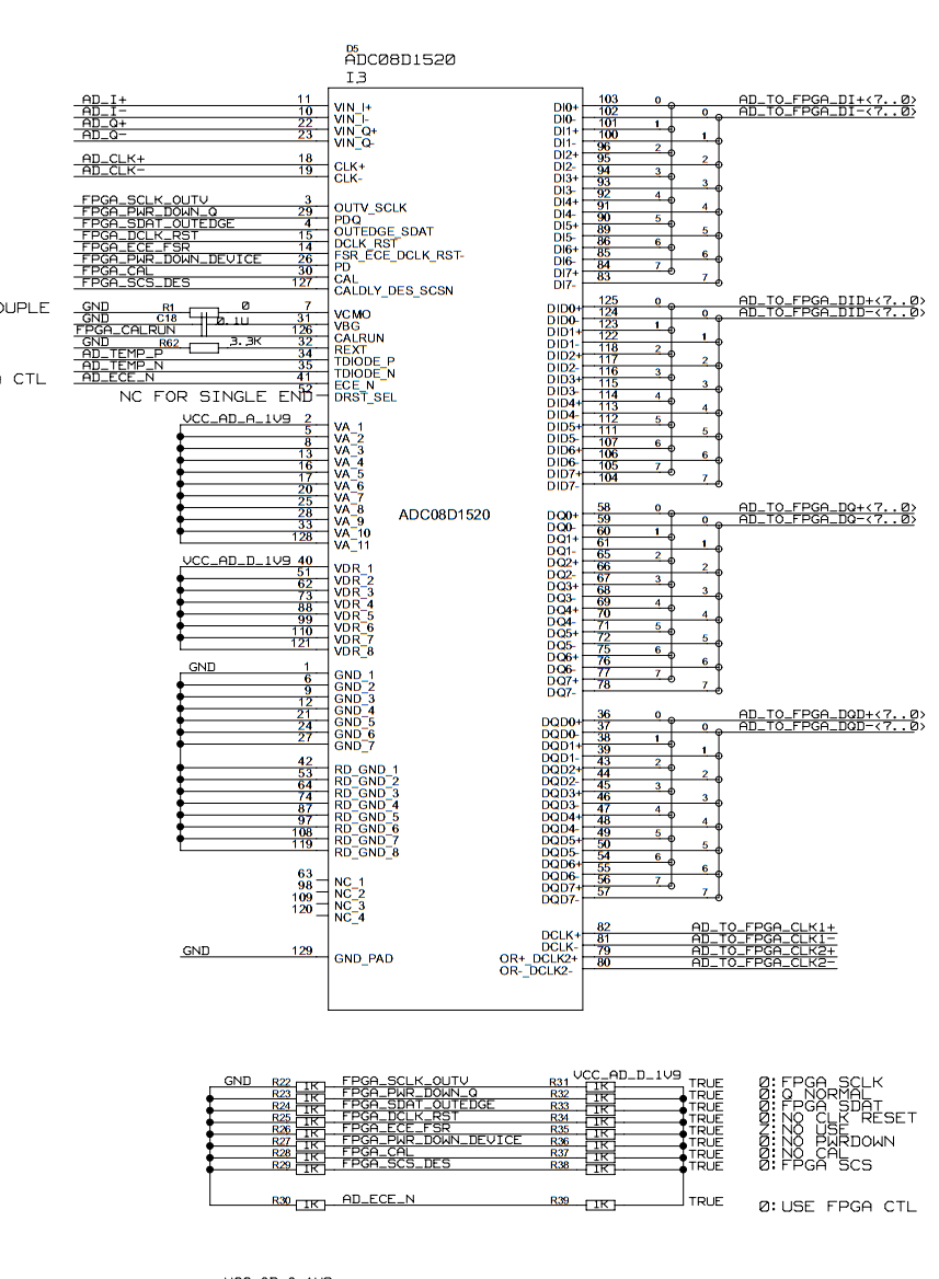
hello ,i try to use FPGA to configure this adc,according to the adc25d1520.v that provided from the forum , i send thte 8 register value through sclk,sdat,scs pin in extended control mde,(pin 41 is low),and set all the other like fsr pin high z. But the sample result is no right according to the FPGA sample data,the sampled data is always 8'h7f or 8'h80/81 when i did not connect any signal to the I/Q input .

is there anything worong with my configuration? the sample clock is 250Mhz provided by lmx2541 pll,all the 8 regiser value is given as the default value described in the datasheeet.

if it wrong ,what is the right configuration step? i only need to confirm that the adc funtion is right.

thank you.

  • Hi shiqi

    You are seeing the correct output for no input signal. The ADC08D1520 has a differential input, and uses offset binary format for the output data.

    When no input signal is applied, VIN+ = VIN- which is the middle of the ADC range. The mid-code values are 7Fh or 80h.

    Please see this figure below for a more detailed representation of the ADC Transfer Characteristic:


    If you are trying to validate the ADC to FPGA data link, you can also enable the ADC Test Pattern Output (Bit 15 of Register 9h - Extended Configuration Register). That will give a repeating pattern on the data outputs that can be used to validate both basic data capture, and sample ordering.

    Best regards,

    Jim B

  •  thank you,Jim B.

    When i enable the  adc test pattern,the output change as described in the datasheet,but the DQ_d channel output is different form the data in the datasheet(it should be FE 01 01,not FE 01 03).It seems that the FPGA configuration timing is right since the test pattern is enabled.

    now my problem is when i input a sine signal ,such as 1MHz, the result i get from the FPGA is still 8'h80/81/7F. The input signal is received form SMB interface,i can get the input signal form oscilloscope.

  • Hi shiqi

    The ADC should not output the 03 value you are seeing on DQd. If you disable Test Pattern Output and apply a signal, you should see that signal represented in the output data.

    Can you send me the schematic showing your input signal path from signal connector to ADC inputs and all other ADC connections?

    Please confirm you are setting the logic level of the following ADC input pins:

    PDQ, PD, CAL, DRST_SEL.

    If you have an AC coupled input, please confirm the Vcmo pin is connected to 0V. If your input signal is DC coupled then the Vcmo voltage should be used to set the common mode votlage of the driving circuitry.

    Best regards,

    Jim B

  • Thank you ,Jim B.

    These are the sch of the adc.The resistence of R31to R39 do not exist,so the control pin are connected to  ground if not configured by FPGA.I set all these pins high Z,according to the FPGA source file provided by the forum,except the sclk,sdat and scs pin.

     the input signal is ac coupled and the Vcmo pin is grounded.

    Should i set the PDQ, PD, CAL, DRST_SEL logical high or logical low?

  • Hi shiqi

    Thank you for the schematics. I don't see any real issues, but the balun you have in the input signal path has a usable bandwidth from 880 MHz to 960 MHz. It will not pass signals that are significantly below or above this frequency range. That is why your 1 MHz test signal did not give a response at the ADC outputs. You will need to find a signal source that can output a sinewave that is between 880 and 960 MHz, or change your balun to a different model that can handle lower frequency signals.

    http://www.tdk.com/s_details.php?class_code=TJA743&item_roots_key=HHM1523C1C06015231&item_name=HHM1523C1

    PDQ, PD and CAL should all be set to logical low.

    DRST_SEL can be left open circuit, or held to logical high. This configures the DCLK_RST circuitry to use the single ended input. If you only have a single ADC08D1520 you will not need to use the DCLK_RST feature anyway.

    Best regards,

    Jim B