This thread has been locked.

If you have a related question, please click the "Ask a related question" button in the top right corner. The newly created question will be automatically linked to this question.

ADS131E04 DRDY stop pulse

Other Parts Discussed in Thread: ADS131E04

Good day!

I am using the ADS131E04.

Blue - CS

RED - DRDY signal after opto

ADC.pdf

  • Hi Artem!

    Welcome to the e2e forum! Thanks for using the ADA131E04! Do you have a question about the DRDY signal?
  • Hi Tom! Thank you for the quick response!
    Problem: pulse DRDY stop without "STOP" cmd
    Sequencing :
    1. RESET pin pull-up
    Pause 10ms
    2. Send SDATAC cmd
    Pause 5ms
    3. Check ID - Read 0xD2
    Pause 10ms
    4. Write CONFIG 3 (0xE0)
    Pause 10ms
    5. Write CONFIG 1 (0x91)
    Write CHnSET (0x10)
    Pause 10ms
    6. READ CONFIG 3 (0xE1 - why? if write 0xC0 - read 0xC0)
    READ CONFIG 1 (0x91 )
    Pause 10ms
    7. Send RDATAC cmd
    Pause 5ms
    8. Send START cmd
    Pause 2ms
    9. Read data 16 time's (3 DRDY pulse skip, on the fourth DRDY pulse)
    Pause 5ms
    10. Send STOP cmd
    Pause 50ms
    GO TO (8)
  • Hello Artem,

    First of all, don't worry about the last bit in the CONFIG3 register. It is a "don't care" bit.

    Let me clarify. Are you saying you consistently read 3 samples of data but the 4th is missing? What could be happening is that your routine to shift the data out could be taking a bit too long and the 4th DRDY never occurs because SCLK is still toggling from the last sample. Please check your interface timing to ensure this is not the case.

    Regards,
    Brian Pisani
  • No.
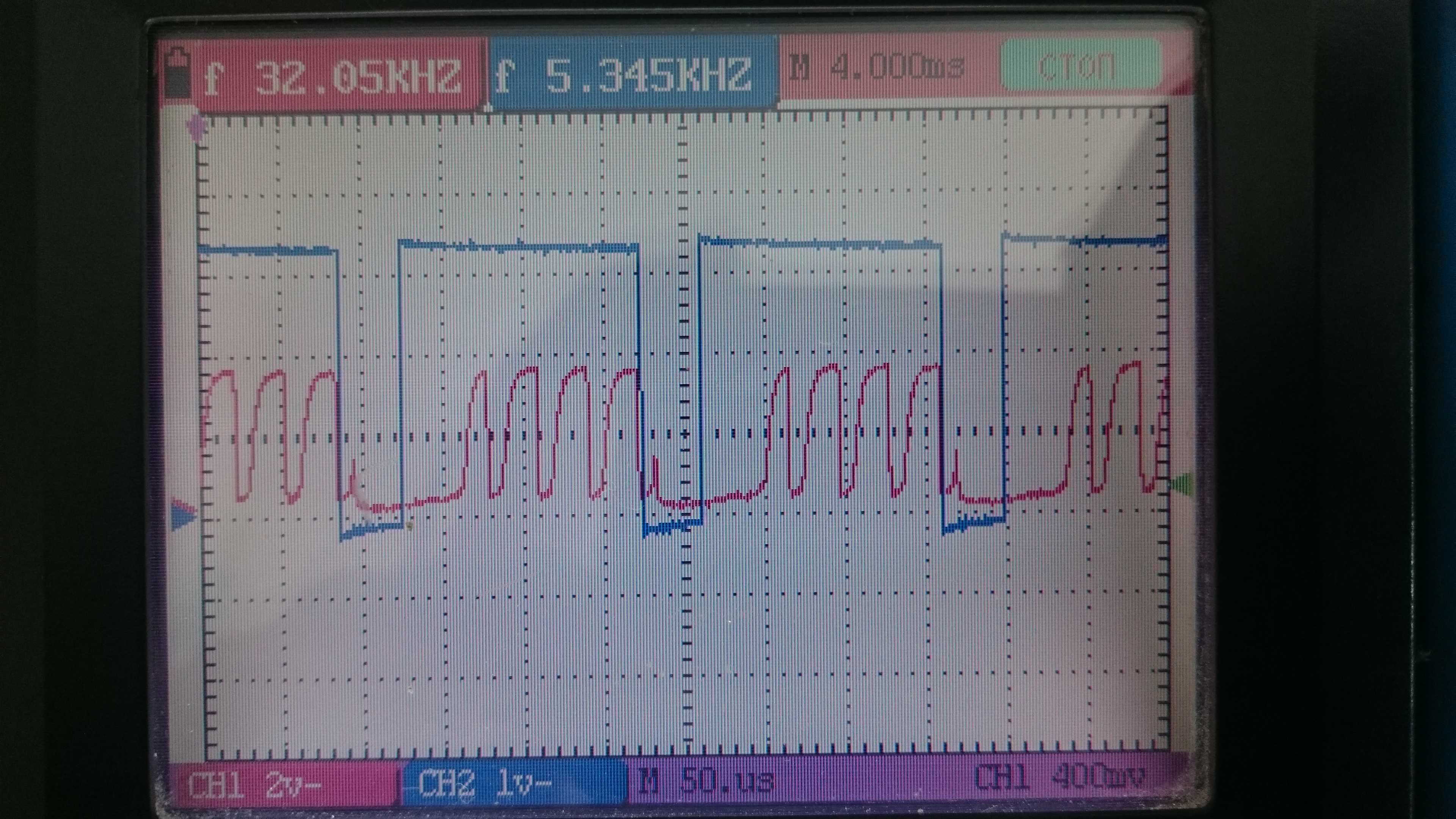
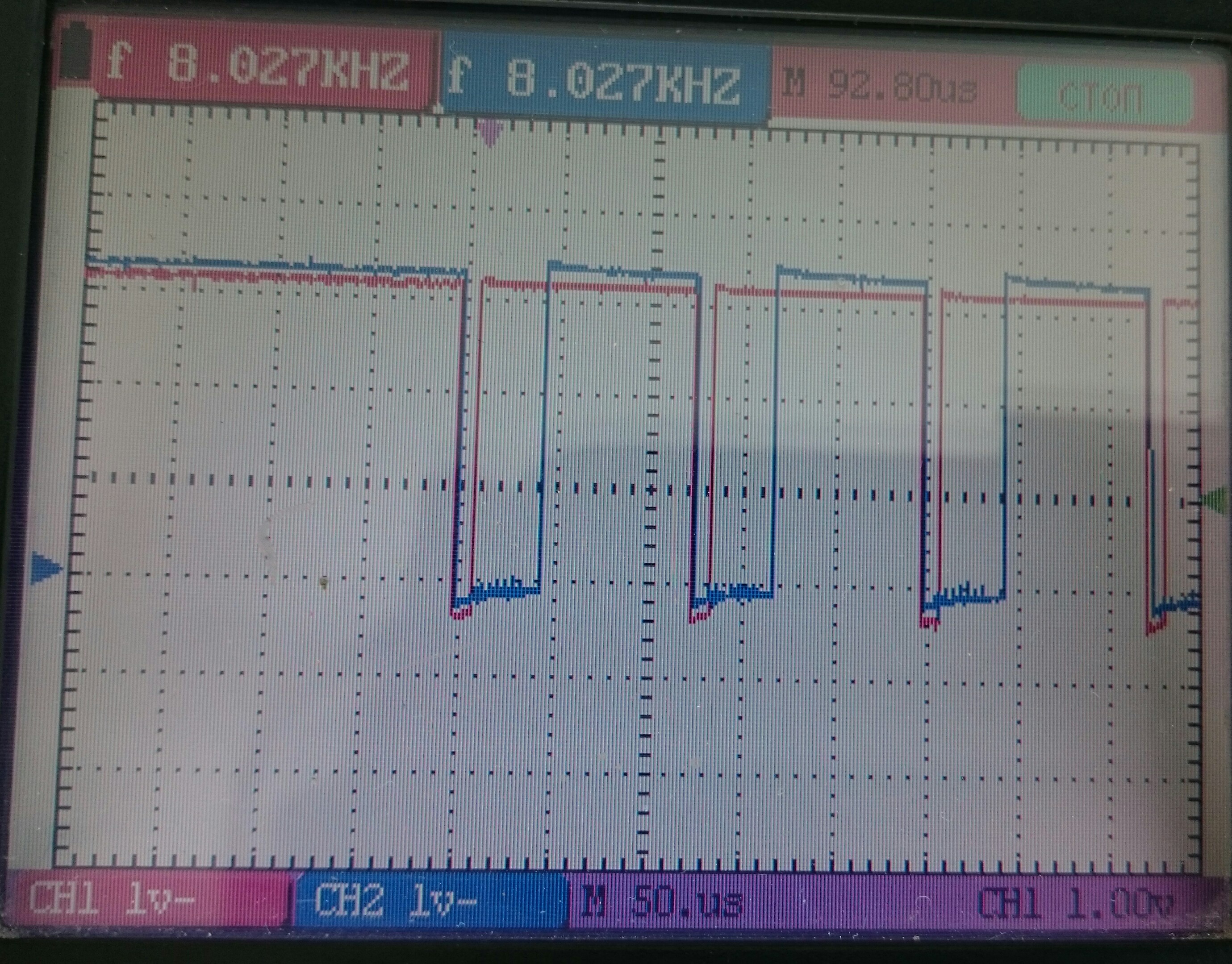
    3 sample skip for data processing (see first post). After several read DRDY pulse stop. If I set 1kSMP problem still.
    I start reading on rising edge DRDY (rising ADC side -> falling after opto as oscillogram into first post ). Is it right? Or must wait for the second edge DRDY pulse and starting SCLK reading?
  • Hello Brian!
    my sequence correct?
  • Hello Artem,

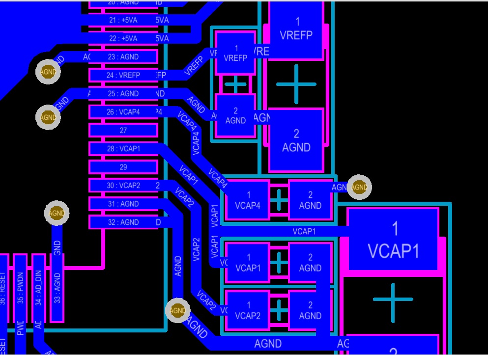
    The sequence seems fine. I did notice something in your schematic that could explain this behavior. It looks as though the RESET signal is driven via optical isolation where, when the host deasserts the signal, the diode is off, the photo npn is off and the RESET pin is floating. When the host asserts the signal, the diode activates, the transistor turns on, and the RESET pin goes low. There is never a scenario where the RESET pin is actively asserted given there is no pull-up resistor. Am I analyzing the schematic correctly? if RESET is not actively asserted, it could cause the chip to go into the reset state intermittently.

    Brian
  • Good day, Brian.

    Resistor R5 10k pull-up RESET PIN

    I changed the optocoupler , and now have a better picture, but problem still.

    red - DRDY (ADC side)

    blue - CS

  • Also, even if not stop DRDY, I reading incorrect values
    (for example, all data 0x00) and sometimes change DRDY freq by default (4kSPS -> 32kSPS )

    The problem does not occur if the input signal is not supplied. whether the correct connection INnN to AGND?

    I removed reset opto and now RESET pin always pull-up.

    1. Send RESET cmd
    Pause 10ms
    2. Send SDATAC cmd
    Pause 5ms

    3. Check ID - Read 0xD0
    Pause 10ms

    4. Write CONFIG 1 (0x95)

    Write CH1SET (0x10)

    Pause 10ms


    5. Write CONFIG 3 (0xE0)
    Pause 10ms

    6. READ CONFIG1 and CONFIG3 
    Pause 10ms

    7. Send RDATAC cmd
    Pause 5ms


    8. Send START cmd
    Pause 5ms

    !!!NOT DRDY pulse ( DRDY once set high ~2ms and set low)


    9. Read data 16 time's  - unsuccessful (not DRDY pulse)

    Pause 5ms

    10. Send STOP cmd
    Pause 50ms
    GO TO (8)

    Why not DRDY pulse?

  • Hello Artem,

    The fact that the data rate sometimes switches back to default seems to suggest that some sort of reset event is happening. Would you mind probing the following voltages when the device stops responding?

    AVDD
    VREFP
    VCAP1
    VCAP2
    VCAP3
    VCAP4

    Thanks!

    Brian
  • Parameters when Input signal not plugged:

    AVDD = 5.4V

    DVDD = 3.28V

    Vref  =  3.92V

    Vcap1 =1.12V

    Vcap2 =2.68V

    Vcap3 =7.4V

    Vcap4 =1.92V

    Parameters when Input signal is plugged to channel 1:

    AVDD = 5.4V

    DVDD = 3.28V

    Vref  =  0V

    Vcap1 =1.12V

    Vcap2 =2.68V

    Vcap3 =7.4V

    Vcap4 =0V


    The first measurement is usually correct. After parameters is left (Vref, Vcap4).

    Vcap4 - ceramic capacitor 1mkF

    Vref  -  ceramic capacitor 0.1mkF and tantalum capacitor TYPE A 10mkF

    what could be causing this?
  • Hi Artem,

    I've just noticed that your AVDD = 5.4V is out of the ADS131E04 recommended power supply specs!

    KR,

    Mo.

  • hm.... power supply provided by DC-DC (P6BU-0505) converter +LC filter. Output voltage is higher than the input... I will fix it.
  • I stabilized the parameters.
    Power supply via 3.3V linear regulator. On one channel ADS131 power supply voltage through resistive divider.
    The problem still.
    Please give me an example PCB design, if possible.
  • Hey Artem,

    The schematic at the end of the EVM User's Guide shows how the EVM is built (www.ti.com/.../sbau200b.pdf). Are you using a different IC from the one on the board that was receiving the voltage over the absolute maximum? That one may have been damaged.

    Regards,
    Brian Pisani