This thread has been locked.

If you have a related question, please click the "Ask a related question" button in the top right corner. The newly created question will be automatically linked to this question.

ADS1232 offset/noise issue

Other Parts Discussed in Thread: ADS1232

Hi Bob,

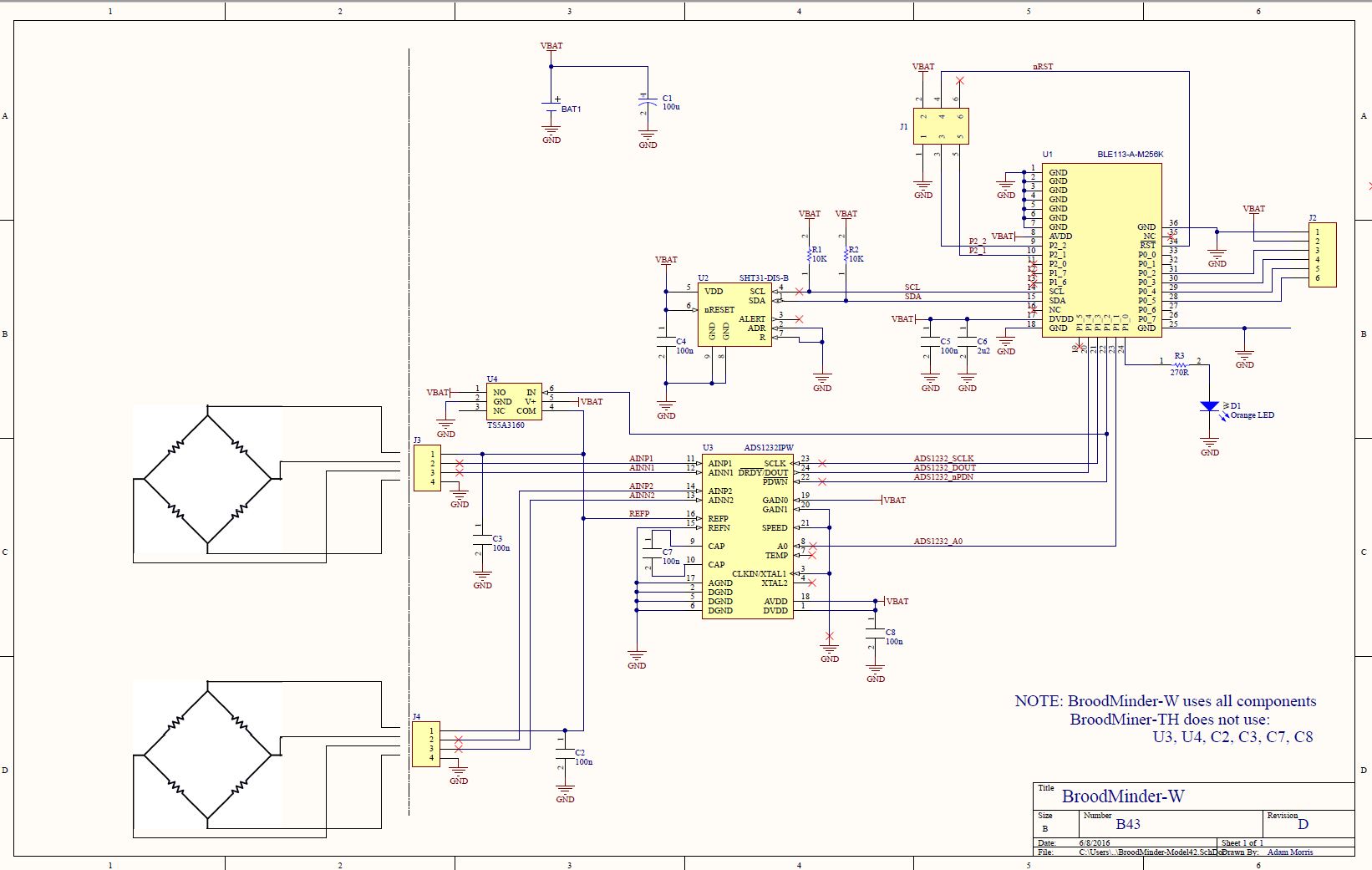
I've been working with the ADS1232 and everything has gone well until I started production. Most of the systems work great. However, I have a number of systems (5-10%) that exhibit a very large offset on one channel or both, on the order of 1,360,000 (btw, it is not railed, it still changes with input). The problem is sort of binary in as much as it is either a wild number, or normal. Nothing in between.I have chased it down to the following possibility and hope you can give me some feedback.

1) Perhaps the no clean solder remnants. I found that as I was attaching wires to in particular pin 8, the problem would go away on a lot of the systems. This actually solved the problem on about 15 systems. A bit un-nerving... I'm thinking that the heat is causing the flux to pool and not 'connect' the pins.

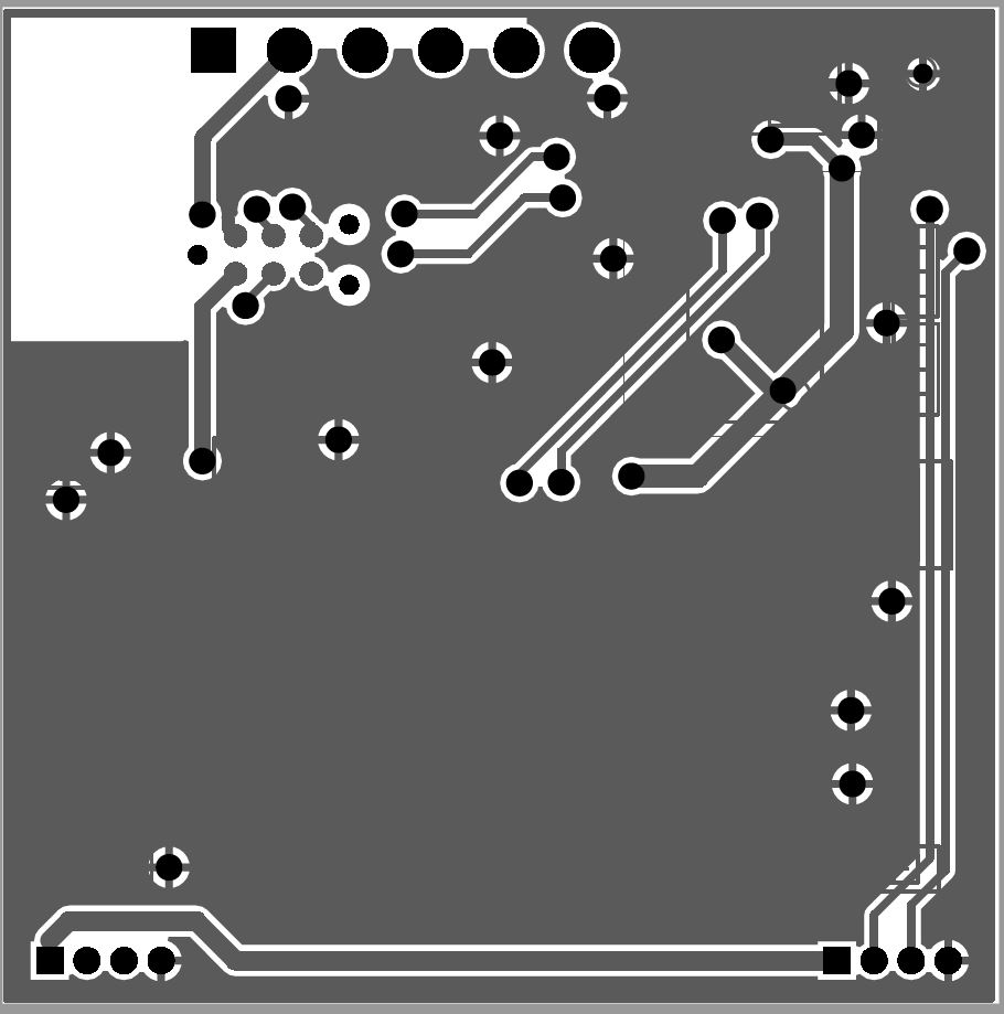
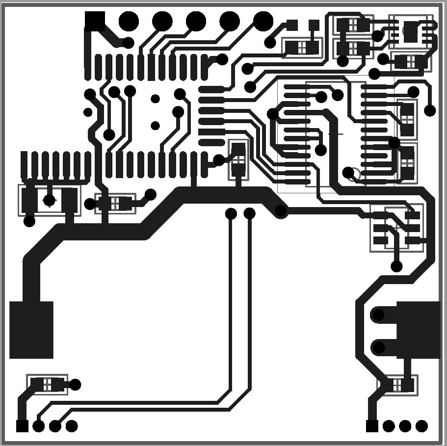
2) Frankly, I'm stumped as to other possibilities. I tried to make the layout tight with good a good ground plane. I tried to use adequate decoupling. The prototypes all worked fabulous.

The gain is not running very high because the sensors I am using (FX1901 from Measurement Specialties) have a large output. I've matched the ranges.

I perform a zero each time before I read the ADC. (Zero, Read channel 1, Read channel 2, repeat) and I have checked to make sure that there is adequate time to complete the cycles.

I have experimented with tacking on extra caps and wires trying to quiet things down, but for a couple of systems, I can't seem to make any headway. The last clue is that if I press on the components near pins 5-10, I can make things happy. I presume some aspect of the loading or cross connection caused by my finger is stopping some oscillation. It does not seem to be a function of voltage. I can use batteries or power supply with the same results.

Here are the details. The battery is a CR2032 coin cell. Thanks for any advice.

  • Hi Rich,

    I hear you had a chilly Syttende Mai this year. 

    Thanks for the amount of detail you've shared regarding your board.  As far as your design, it is difficult to say what might be the difference between the prototypes and production boards.  I can tell you that the nodes around and at pins 9 and 10 are very sensitive. Your C7 is connected to these pins and I will assume is multi-layer ceramic.  MLCC caps can have a peizo effect that can add noise, especially when stimulated by vibration.  The best cap to use is some type of poly film.  If you must use MLCC for size reasons, then the highest grade of cap should be used and preferably C0G/NPO.  On the boards you are still seeing issues, you might try replacing C7 with a higher grade of cap.

    That said, I doubt this is the cause of your large offset unless there is a connection issue.  It almost seems that you are seeing an inverse response like if you switch +/- inputs.  This may be difficult, but is there are way that you can show me the result codes from the ADS1232 for both the expected value and the failing value?

    In general I don't like to rely solely on EMI/RFI filtering that takes place when the external filter cap (C7) is the only low pass filter. Any high frequency content that is input into the ADC can still cause issues internally, so I like to use an external low pass filter to knock down the noise prior to the ADC.  From the looks of things, your biggest source of RFI is from the Bluetooth module on the board that can be picked up by the long input traces and sensor wiring.  If this were the culprit it should also show on your protos.  Also, the reference might be improved by having a cap closer to the ADC reference inputs.

    These are all suggestions on performance improvements and do not specifically address the problem you are seeing.  You mentioned connecting wires to pin 8 and some boards started working.  You also mentioned flux.  Were you boards manufactured via a reflow process?  Are you using a lead-free solder?  I would examine the joints carefully around the sensitive nodes and C7 in particular.  Make sure all joints show good flow and no 'cold' joints.  One problem with using no-clean flux and lead-free solder is making sure that the reflow cycle is hot enough to activate the flux fully during reflow.  Also, if solder paste is stenciled incorrectly or if there is too much time between stenciling and reflow there can be issues.  High tin content plating can also cause connection issues due to oxidation. The results of these types of issues should be observable under a microscope observation of the joints.

    Best regards,

    Bob B

  • Thanks for the quick response, yes Syttende Mai was pretty awful weather. You must have some inside information. ;-) The actual 17th of May was lovely. I guess we shouldn't have rushed it those 3 days....

    Thanks for the great feedback, I'm glad you didn't say there were lots of layout issues or that something was horribly wrong. At one point I was afraid I was blowing out the chips... which was crazy, but until you figure out what is wrong, your mind assumes the worst.

    I'll try the poly film although I would be surprised if vibration were a problem. Certainly on my bench things are quiet (except for my own personal shakes...)

    Are the result codes passed in the data after Offset cal? I can add reading them to the software if it will tell us something. Are they secret TI things or can you share?

    I'll try the reference cap also. I did worry about that some since it is hanging out at the end of the trace...

    I tried shorting the inputs and still had the problem, so I'm inclined to discount filtering, but I will test this again... The output resistance of the strain gauge is in the 2K range, so I wasn't expecting big noise problems. Additionally, this is a beehive scale (broodminder.com)environment to be pretty quiet.

    I'm stopping by the CM house today, so I'll check on the reflow. They do a great job in general, so I don't expect that to be a problem either.

    Of course, that means I don't expect any of this to be a problem... but something is. I'll keep turning over rocks until it is found.

    Thanks, Rich
  • Well, I tried several things to no avail on one particular board.

    resoldered all pins
    shorted inputs
    removed strain gauges completely (with their 6" of wire)
    removed c7
    replaced c7 with 1 uf mlc (I don't have any poly)
    Nothing fixed the issue

    However, If I add my index finger to the mix, pressing in the area of c8 and pins 1-8 I can make the problem go away by pressing hard enough. I'm not sure what all I'm contacting...it includes a bit of U4 too... I know that it is not mechanical because I don't get the same response with a plastic 'finger" press.

    ??
  • Is it possible that the problem is due to the TEMP pin floating. I don't see that the data sheet mentions it other than to set it high...
  • Hi Rich,

    I'm sorry I didn't catch that in the schematic.  A floating digital input pin could float to any value, and it can also cause excessive current draw.  If you are not going to use this mode you should tie it to GND.  So yes this could be the issue.

    Best regards,

    Bob B

  • Oh goodness...it is sometimes simple... I guess there is no pull down on the TEMP pin, so grounding it made my troubles disappear... Lucky that it is an easy rework.

    In general the datasheet is good at telling to leave open or tie... I didn't use the TEMP feature, so I did not read close enough to see it was just a mux control and should be tied. I suggest that note get added for those of us who don't notice...

    That is assuming that you agree this is the likely problem.

    Cheers
  • Hi Rich,

    I deleted your schematics/layout from the public post. I'm glad the resolution was simple.  Feel free to ask if you have any further issues.

    Best regards,

    Bob B