This thread has been locked.

If you have a related question, please click the "Ask a related question" button in the top right corner. The newly created question will be automatically linked to this question.

ADC12D1600 - DCLK level while DCLK_RST asserted

Other Parts Discussed in Thread: ADC12D1600, ADC12D1600RF

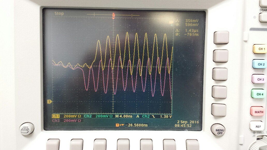
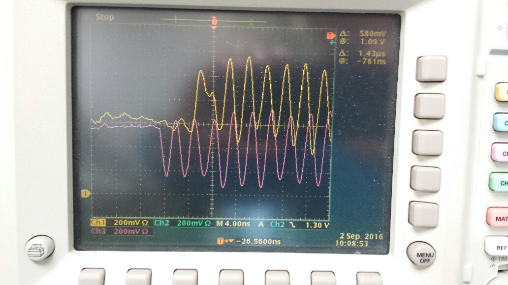
I'm using the DCLK_RST functionality of the ADC12D1600.  I begin by writing bit 0 of address 0xE to0 to enable this functionality.  I then generate a synchronous dummy reset pulse (high for 3000 sample clock periods) on DCLK_RST.  Finally, I generate another reset pulse on DCLK_RST.  I have noticed that while this second reset pulse is asserted, the ADC DCLK output will stop either low or high. Is this expected? I thought the DCLK was supposed to come out of this second reset in a known way.

  • Hi Mike

    The DCLK output should transition to logic low when DCLK_RST is asserted. This should occur after tSYNC_DLY input CLK cycles plus tOD logic delay.

    Can you try putting a longer delay in between your synchronous dummy reset pulse and the final reset pulse you are using to perform the actual device synchronization? How long is the current delay between these two pulses being high?

    Best regards,

    Jim B

  • Hi Jim,

    The delay between the pulses is greater than 4 microseconds.

    I should mention that I'm using 1:4 Demux DES mode.

    Thanks,

    Mike

  • Thanks Mike

    I reviewed the documentation again and I had the polarity wrong, the DCLK outputs should be high while DCLK_RST is captured as logic high.

    I'm getting a bench setup together to look at this but haven't quite got things together yet. In the meantime I have a few more questions about your design and usage:

    • Is your input CLK AC coupled?
    • Is the CLK frequency constant and stable while you're applying DCLK_RST?
    • Have you changed any register settings other than the one bit to enable the DCLK_RST feature?

    I hope to have some information from my bench setup soon.

    Best regards,

    Jim B

  • Hi Jim,

    The input to the ADC is AC coupled.  It is a constant, stable 1.5 GHz for at least 4 us prior to the register writes, and thereafter.  The register writes are...

    write addr  0 with 0x20a0
    write addr 14 with 0x0002

    The register writes are immediately followed by the dummy reset pulse, then another > 4 us period, then the actual reset pulse.

    In writing this, it occurs to me that maybe I should add some additional delay between enabling DCLK_RST and the dummy reset pulse?  It's possible that is only 100s of ns.

    Thank you.

    MIke

  • Hi Mike

    My very preliminary results applying a static DCLK_RST input show that the DCLK outputs do stop in the same state consistently.

    There are some advanced blocks in the clock path that perform duty cycle optimization for the DES mode of operation. Those may take longer to setting than the 4us you mention. Please try ensuring the clock is stable for at least 50ms before doing the DCLK_RST procedure.

    I agree that you should also increase the delay between enabling the DCLK_RST and applying the reset pulses. I'm not sure how long this path takes to stabilize, but I would give it 1ms as a first test.

    Best regards,

    Jim B

  • Hi Jim,

    I'm looking at this again after a long distraction.  I'm seeing the DCLKQ output at a logic low while I apply DCLK_RST rather than the expected logic high.  And when it resumes, the first high pulse is sometimes a full period rather than the normal half period.  I was looking through the register values to see if anything looked out of place.  I noticed that several of the reserved registers (i.e. addr 1, 6, 8) have different values than the POR values listed in the datasheet.  Would anything in these registers explain the behavior that I'm seeing?

    ADC Register at address 0 = 0x20a0
    ADC Register at address 1 = 0x2907
    ADC Register at address 2 = 0x0000
    ADC Register at address 3 = 0x4000
    ADC Register at address 4 = 0xdb4b
    ADC Register at address 5 = 0xfbfb
    ADC Register at address 6 = 0x1c2e
    ADC Register at address 7 = 0xc142
    ADC Register at address 8 = 0x0f0f
    ADC Register at address 9 = 0x0000
    ADC Register at address 10 = 0x0000
    ADC Register at address 11 = 0x4000
    ADC Register at address 12 = 0x0004
    ADC Register at address 13 = 0x0000
    ADC Register at address 14 = 0x0002
    ADC Register at address 15 = 0x001d

    Thanks,

    Mike

  • Hi Mike

    If you're not writing to those reserved register addresses I don't think they will be causing a problem, though I will double check what I see in my setup.

    Have you tried just leaving the ADC clock on constantly, so it has been stable for a long time before the register writes and application of DCLK_RST?

    If things work OK with long delays (as I have in my setup) then you can try shorter delays again.

    Best regards,

    Jim B

  • Hi Mike

    All of those reserved register values are correct for the ADC12D1600RF device.

    I tested on the bench with your settings and I see DCLK stop consistently at the same level. Please let me know how testing goes with the clock continuously applied and the device stable for at least 5 seconds before DCLK_RST is applied.

    Best regards,

    Jim B

  • Hi Jim,

    Thanks for checking the register values.

    The sequence of events is this: First, we do stop the clock for about 1us so it can come up with a known phase with respect to other clocks on the board.  After that, I believe it runs continuously.  Next, we put the ADC in DESIQ mode and set the DES Timing value and finally enable the DCLK_RST function.  After that we issue a "dummy" reset to the ADC and then another reset. 

    I've added pauses prior to each of the two resets which wait for me to press Enter.  Even with these pauses, I am still often seeing the DCLKQ output resume toggling with an odd duty cycle in the first cycle -- like a full period high then normal half period low.  I can attach some scope plots if there is a way to do that.

    Assuming the ADC CLK is stable, which I believe it to be, is there anything we might be doing wrong on the DCLK_RST input which might explain the observed behavior on the DCLKQ output?  Not meeting setup or hold, for example?

    Thanks,

    Mike

  • Hi Mike

    The setup and hold timing is the only thing I expect should affect the behavior.

    You can attached screenshots or other files in E2E. On your next reply, click on the "Use rich formatting" text below the right side of the text entry field. In that mode there are a number of formatting and attachment tools available to embed images or attach files.

    I'll see what I can do to replicate your timing using a different clock/DCLK_RST source. I'm not sure if what I have is flexible enough but I'll let you know if I can get any results from that setup.

    Best regards,

    Jim B

  • So here is the ADC DCLKQ+ output, in the yellow-ish color, when it resumes following the deassertion of DCLK_RST.  I believe we are looking at the positive side of the differential signal here.  The other clock in the pink-ish color is the output clock of a DAC which gets a copy of the same reset.  Anyway, this is the "good" case. 

    Here is what it looks like in the "bad" case, which I see about half the time.  Notice the strange double-hump at the start.

    I believe the CLK input to the ADC is a stable 1.25 GHz at this at this time, but it's entirely possible we are messing something up with the DCLK_RST signal.  I believe that signal is being asserted for 500ns, or 625 periods of the ADC input clock.

  • Hi Mike

    I've managed to cobble together a test setup that allows me to apply CLK at 1.25 GHz along with a periodic DCLK_RST pulse and sweep the skew between CLK and DCLK_RST.

    With the same settings you are using everything works fine with the proper alignment of CLK to DCLK_RST. It is possible to adjust the alignment of CLK and DCLK_RST into a range where the transition from the DCLK reset state to the active state is unpredictable, or has a longer than normal initial DCLK period. As long as I keep the CLK to DCLK_RST timing outside that range everything looks good.

    You should review your circuitry which generates DCLK_RST as a function of CLK to confirm the alignment will be consistent, and should meet the setup/hold specifications.

    Best regards,

    Jim B

  • Jim,

    Thank you for taking the time to reproduce that.  The buffer that we are using to drive the DCLK_RST is highly configurable, but it has some idiosyncrasies.  There may be a way to create a more predictable pulse on DCLK_RST by actually creating two pulses, the second of which would be high for 625 periods of the 1.25 GHz clock, starting 625 periods after the first.  Any problem that you're aware of with having two reset pulses this close together?

    Thanks,

    Mike

  • Hi Mike

    That should work fine. 625 clock periods is ample time. The ADC will see 2 DCLK_RST events separated by around 625 clock periods. The timing of DCLK_RST to CLK on the final event is the most critical, in particular the capture of the falling edge of DCLK_RST.

    Best regards,

    Jim B