This thread has been locked.

If you have a related question, please click the "Ask a related question" button in the top right corner. The newly created question will be automatically linked to this question.

DAC7578 Address issue

Other Parts Discussed in Thread: DAC7578

To sum up: DAC7578 is responding on the wrong address and appears to be doing so independent of what the address pins are pulled to. This happening to only a subset of boards and has been fixed by replacing the DAC. I'm looking for some sort of smoking gun or possible root cause, possibly some sort of advice for our contract manufacturer if this related to assembly/handling.


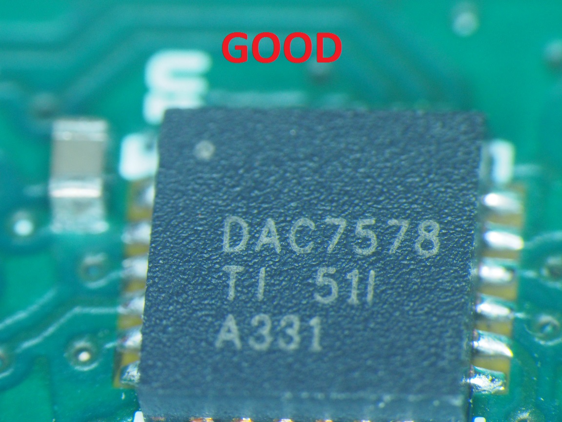
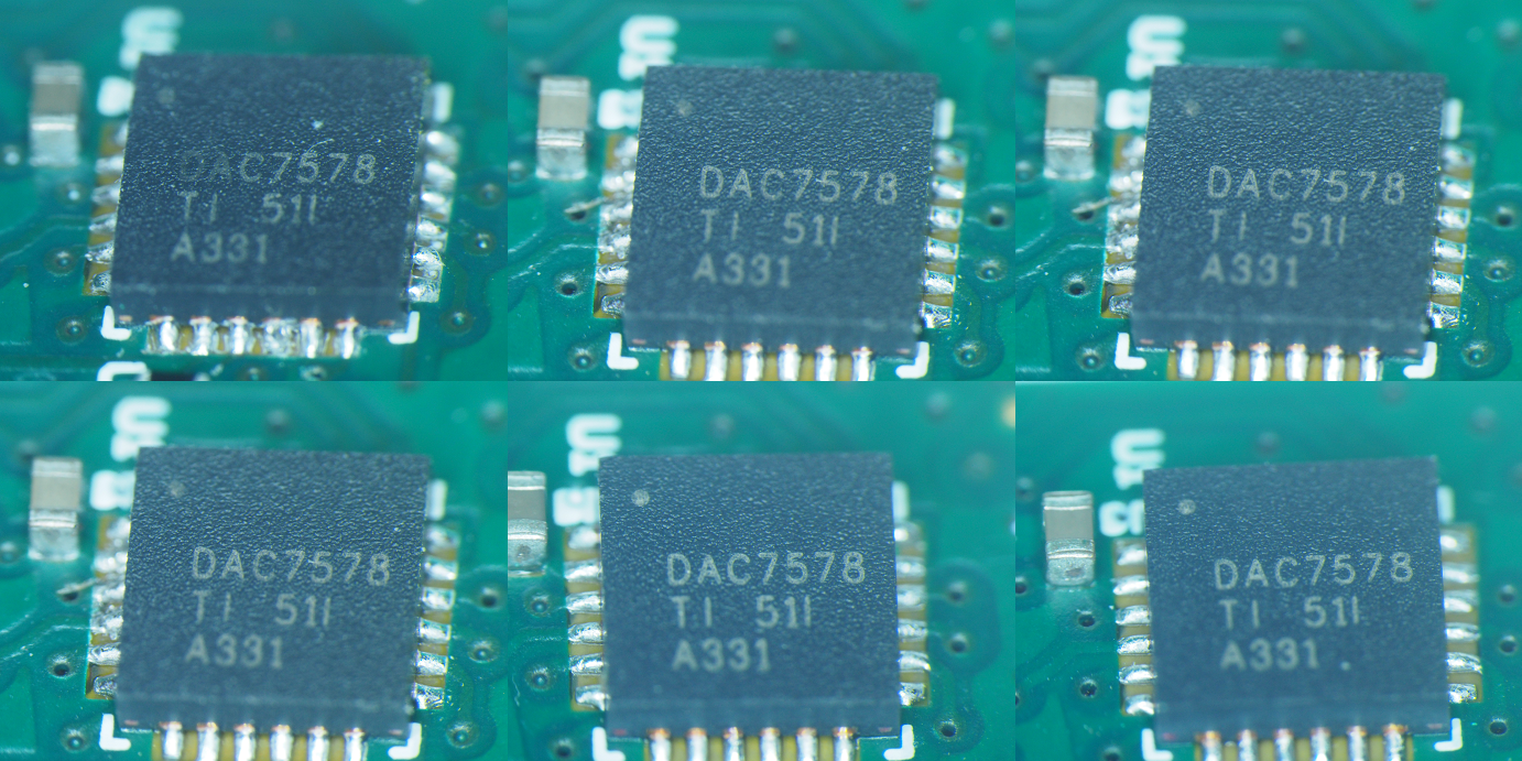
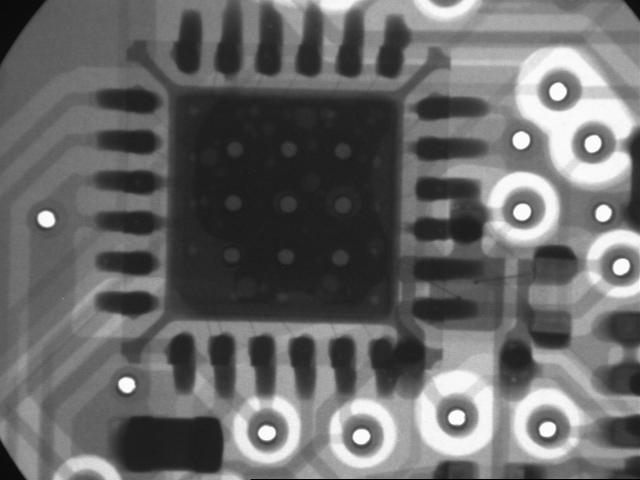
I've built ~100 boards with the schematic/layout detailed below and on a large potion of them DAC7578 behaves as expected, however on a subset of them (~10) it appears to just not respond on I2C. Continuity checks on I2C data/clock show a good connection, visual and xray inspection of the parts show no skew or shorts. 

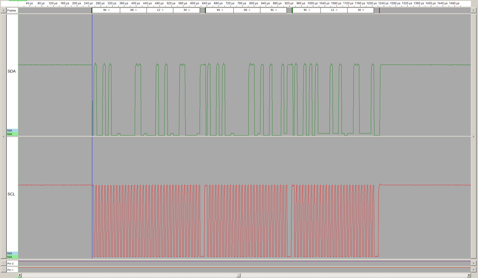
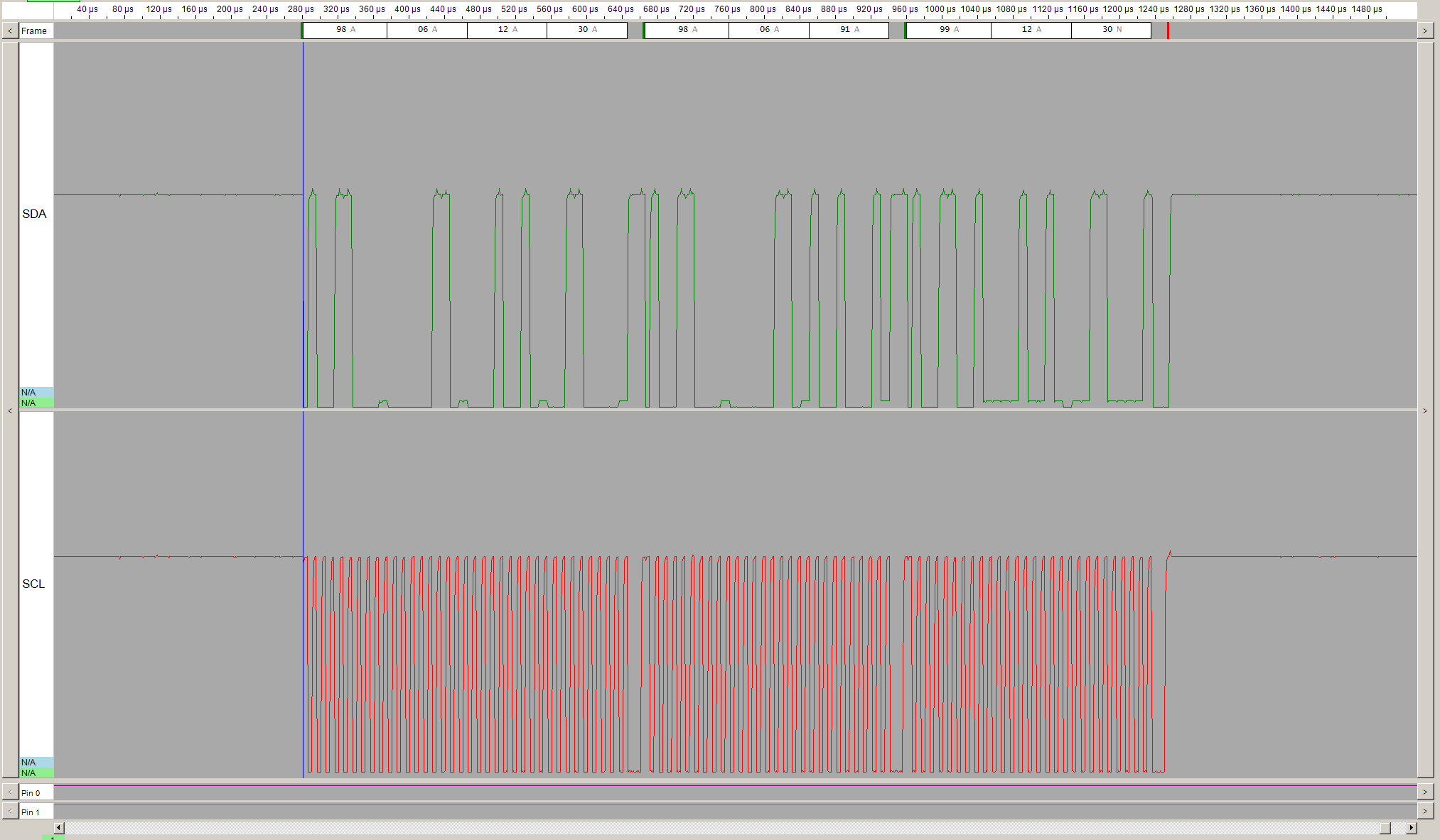
While troubleshooting I decided to try all of the possible addresses that the DAC could be on and I found that the part was responding on the wrong address! The expected address with Addr0 = 0 and Addr1 = float would be 0x4C, on 3 different failed boards I was getting a response on 0x4A instead. This is an address which would be consistent with Addr = 0 and Addr1 = 1.

This is in a test setup where the only I2C device on the bus is DAC7578 and I am using a telos XL2.0 I2C debugger. I am sending a 123 into the 6th channel buffer and then attempting to read back that buffer, 0x4C NAKs, but 0x4A gives the correct response. 

The next thing I checked was what would happen if I pulled down Addr1, in case there was some slightly lower impedance pulling it up internally-

It should respond on 0x48 with Addr0 and Addr1 = 0. There device NAK'd and continued to communicate on 0x4A.

Here is the schematic and layout of DAC7578.

On the board layout there are no pins adjacent to Addr1 that could have bridged solder and pulled it up, every adjacent pin is GND. The via closest to it is -20V and is not bridged.  As mentioned before, visually the chip appears soldered correctly with no skew.

There is no correlation with the datecode of the parts.

  • Howdy James,


    And welcome to the e2e forums! Thank you for the post and information, we will review and get back to you as we obtain more information on this matter.  In the meantime, can you possibly supply us with an oscilloscope capture of this issue?

    Best Regards,

    Matt

  • Using the I2C ADC in lieu of a scope for expediency- I can get high res scope traces if you need  them.

    Below: 0x4A communicating normally

    Below: 0x4C NAKing

  • For reference, here is the same command working on 0x4C on a "good" board:

  • Howdy James,


    Is it possible to provide a picture of the AVDD pin when power is applied? If the supply is not brought up linearly there is a small chance that the internal OTP will load incorrect trim values -- this will affect the behavior of the device.

    Best Regards,
    Matt

  • There's nothing too remarkable in the VDD as it comes up on its own, it's running off a local linear regulator

    I have also plotted what SCL and SDA look like when the board powers up, they are powered from a switcher and come up before the VDD regulator comes up.

    C1 is SCL

    C2 is SDA

    C3 is VDD

    This is what the supplies look like when the system is hooked up to debug equipment, the misbehavior happens regardless of the equipment connected, but I'm including it for completeness sake. The system is hooked up through a USB cable and JTAG in this and is drawing some amount of power, which offsets the initial I2C voltages slightly.

    C1 is SCL

    C2 is SDA

    C3 is VDD

  • Hi James,

      Several requests here to help debug this issue.

    First, please get a 'scope capture of SCL/SDA expanded, similar to Fig 116 in the datasheet.  Please move the traces closer together, even superimpose, as I want to see the relationship of the edges.

    Next, are all the DAC7578s of the same lotcode?  All came from the same source? 

    Finally, on a working board, using a DVM, please measure the dc voltage at A0 and A1 in a static state (no i2C traffic) and then do the same on a failing board.

    I believe you said when you replace a failing DAC7578, the board then operates as expected, is that correct? Could you try removing the DAC5758 on a failing board, then replacing it with the same device, see if the problem still exists. . . this would indicate an assembly/solder issue. 

    Thank you,

    ~Leonard      

  • Here are some more scope captures of I2C-

    This is an example of a "good" behavior, responding on 0x4C.

    This is an example of "bad" behavior, NAKing on 0x4C

    This is an example of the same board that NAK'd 0x4C responding on 0x4A:

    • I will try to IR reflow and reseat a part; we don't have the best setup to do this quickly, so this could take a little bit.
    • Lotcode info coming soon
    • A0/A1 info coming soon, it's not easy to get wires onto there.

  • This is a responsive dac from our first batch

    From top left to bottom right are oldest -> newest, with the rightmost 2 in the bottom row coming from our most recent batch. These all have the same issue where they respond on 0x4A instead of 0x4C

  • I don't think I have a DMM with a high enough impedance to measure that floating pin properly.


    On both boards: I froze all I2C traffic after confirming that the good board responded and the bad board did not. I also confirmed after measurement that this persisted.


    On a good board-

    When I measure it with a fluke 115 I see ~65mV on Addr1, with 0V on Addr0.

    It's sitting around 2.5mV when I measure it with a 1M probe.


    On a bad board-
    When I measure it with a fluke 115 I see ~30mV on Addr1, with 0V on Addr0.

  • I am still working on removing and replacing the DAC7578 on a bad board.
  • I have removed and replaced DAC7578 on a board that was only responding on 0x4A, it now responds on 0x4C.

    I am going to try this on a second board to confirm.
  • Removed and replaced a second with positive results.

    Our CM will be xraying some of the failing boards to see if there could be anything slight shorts that were missed- do you have any thoughts on which pins could be getting shorted or possibly marginally connected? - This behavior is inconsistent with what would happen if the address lines were shorted.
  • James,

      Thanks very much for this information and troubleshooting effort - really appreciated. 

    Since the ADDR1 is floating, but acting as if it were a '1'. Since the ADDR1 pin is between the ADDR0 and the RSTSEL pins, and both RSTSEL and ADDR0 are at GND, I'm at a loss of how this pin could be 'pulled-up' to make it look like a '1'.  I'm thinking perhaps excessive flux, or solder whisker, but I don't see where either could come into contact with a non-0 voltage. 

    The only other possibility I can think of is a trace under the pin that is coupling noise on the pin at just the right time so it bumps the open-pin voltage up high enough to look like a '1' at the ADDR CLK time.

    Here's one more experiment.  Take a failing board, powered-OFF, measure the resistance ADDR1 to GND and ADDR1 to VDD, then do likewise on a working board - let's compare.

    ~Leonard 

  • On a good board- 2.11Mohm between ADDR1/GND and ADDR1/VDD with probe negative on ADDR1, 7.92Mohm with probe positive on ADDR1.

    On 2 bad boards- 2.09, 2.10 Mohm between ADDR1/GND and ADDR1/VDD with probe negative on ADDR1, 7.89, 7.90 Mohm with probe positive on ADDR1.

    I had measured these resistances previously; there didn't seem to be any variation of consequence. I confirmed that the RSTSEL was connected too- you can see the soldering in most of the datecode pictures.

  • James,

    Thank you for the information, out of curiosity did you try the swap experiment with multiple devices or with one device? If you tried on multiple devices, did all have positive results when switched to a good board?

    Best Regards,
    Matt
  • So far I have swapped 3 different DACs on 3 different boards. Each board had the DAC removed and replaced with the same DAC.

    EUT1: Began responding on 0x4C, good behavior. I passed it off for assembly/full functional test and the DAC reverted to responding on 0x4A

    EUT2: Began responding on 0x4C, good behavior. I passed it off for assembly/full functional test and the DAC reverted to responding on 0x4A

    EUT3: Just replaced this afternoon, still responding on 0x4A

    Do you have any insight as to what could cause the DAC to be responding on one address, but then switch to a different one with no actual hardware changes?

    My initial guess was some sort of ESD event causing internal biasing the address pin, but that doesn't explain why the problem went away initially on EUT1 and EUT2.

  • I will try to reheat these tomorrow to see if the problem goes away again.

  • James,

      You first tested these on the bench, they worked correctly, then sent to Production Test . . . is the test setup and equipment at Production Test the same as what you were using at Bench Test?  If you retested one that failed at Production Test at your Bench Test, does it still fail?

    ~Leonard 

  • They fail at both locations, our production test uses the same hardware. It had actually been working for them for about a day, and then at some point they notified me because the voltages were no longer coming up- logs showed that communication was failing so I took back the boards to test using my debugger.

    The production test is running a script that performs a functional test using our onboard ADC/reference, then assembles the board into a housing and repeats. 

  • I took the opportunity to do some more testing, and I confirmed that Addr1 does actually operate as expected when I short it to ground on boot. I had been shorting with a probe previously and I must have not been holding it down hard enough.

    EUT1 and EUT2 both respond on 0x48 when I short Addr1 to ground.


    If all else fails I might move our I2C addresses around so we can use 0x48 instead.
  • I tracked down a 10Gohm DMM and re-measured the voltages at the Addr1; a good board was reading ~10mV, the bad boards were reading 15-30mV on addr1.
  • Very interesting . .  wonder where the leakage voltage is coming from . . . if you can easily change the bus address to 0x48 and connect ADDR1 to GND, I would take that approach.  I have never been a big fan of using the 'float' level to add a third state for a digital input.  So a hard connection to GND makes me feel more comfortable with the address reliability.

    ~Leonard   

  • We had 7 boards that were failing xrayed, and all of them showed no soldering defects, this seems to indicate that there is some voltage leaking internally- 

    The shadow is from a pad on the opposite side of the board.

    Could I send any of these parts in for FMA?  If there are any requirements  (part on/off board) please let me know.

    We are planning to switch to a 0x48 address configuration moving forward, but it's not a trivial fix and I'd like to get some positive confirmation on what went wrong in the meantime.

  • Hi James,

      Yes, to initiate an FA, you will have to get the distributor from whom the parts were purchased to start the FA process.  They will have the process and procedure for submitting these for Failure Analysis.  Off-board with proper ESD handling/packing is what will be required.  

    ~Leonard 

  • I've started that process, in the meantime do you have any guidance on the use of floating address pins for this kind of part? is there any expectation of lowered reliability if a floating address pin is used?

    There isn't much info on the datasheet about the float pin specifically, could you get me any information about the power on sequencing of the part and how the voltage at that pin configures the address?
  • I'm wondering what would happen if you add a capacitor to the floating pin, let's say, 100nF?  I'm thinking that there may be some noise, and at the time the address is latched (I believe it is at power-ON ramp time), adding the cap should stabilize the 'float' condition.  Would you try this on a board that is typically failing now? 

    ~Leonard   

  • Hi James,
    My name is Rahul Prakash. I am the systems engineer supporting these devices.
    Were you able to resolve this issue with the suggestions from Leonard?

    Best Regards,
    Rahul Prakash
  • The problem is still happening; our latest batch came in with about the same failure rate (10%), and all with the same mode of failure.

    I have not had time to try reworking on a 100nf yet.

    We have removed 5 and sent them back for FA.

    We are switching our address configuration to not use the float feature on future fabs.

  • Hi James,
    Just curious, did you try the capacitor on the ADDR1 suggestion?
  • Unfortunately I've not had a chance to put that on yet; I'm hoping to get more free time later in the week.