This thread has been locked.

If you have a related question, please click the "Ask a related question" button in the top right corner. The newly created question will be automatically linked to this question.

DAC38J84- SPI Interface

Hello TI,

I had a query regarding DAC38J84- SPI Interface. Can you kindly help me with the same.

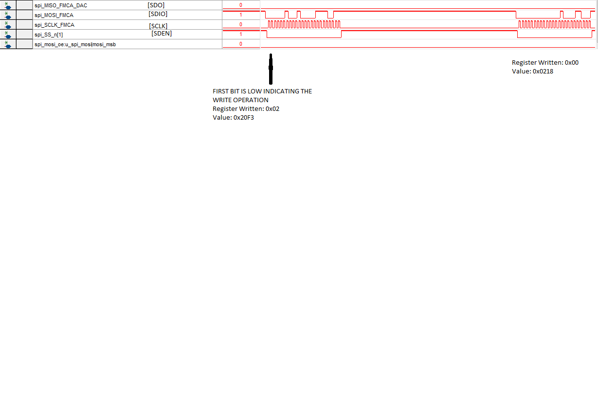
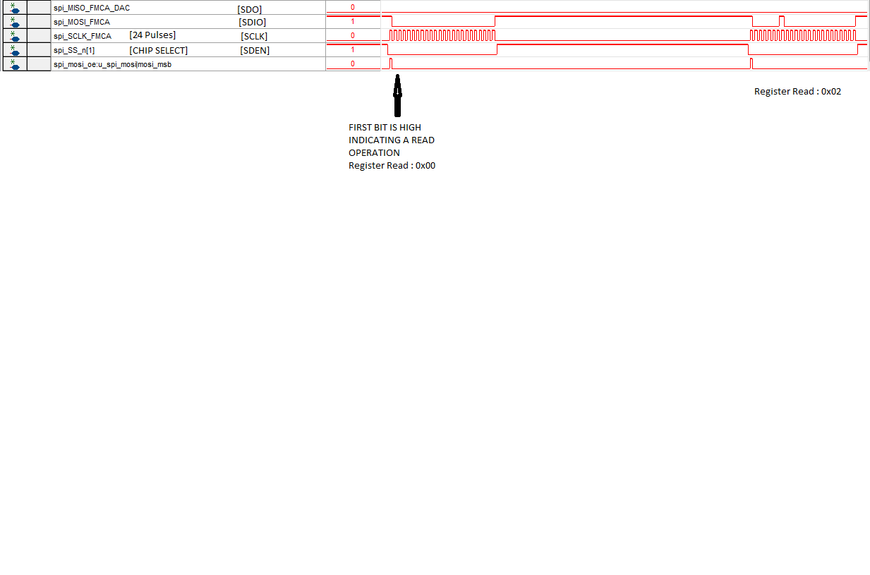
I am trying to configure the DAC chip with SPI 4-wire interface. I initially perform SPI write of all DAC Registers and then try to read some of the registers. I believe the SPI write operation happening effectively as I can see that from the MOSI signal from the scope. But when I try to read few of the registers, I see that the MISO signal remains LOW(0) all the time. I also ensured that I am not reading only the registers with "0000" default/written value. Irrespective of any register read, I see MISO signal to be LOW(0).

I have previously worked on ADC where ADC had a 'SPI_CONFIG' register to set the MISO voltage which controlled its operation. However I don't see any such register mapping or option for DAC. So can you let me know what might possibly the problem to be? Should a Voltage be set for this MISO pin for its operation? If yes, what should be the ideal value or range?

Thanks,

Anuj

  • Anuj,

    You will need to first write to register 0x02, bit7 to enable 4 wire mode. Perform SPI write first to write to the bit, and then read back using 4 wire mode to see if you can read this bit.

    -Kang

  • Hello Kang,

    I have already enabled the 4 wire mode. I am setting the bit 7 of Config 0x02 to '1' while writing the registers. I have tried reading this register after writing as well. I still see LOW(0) in MISO signal.

    Anuj
  • Anuj,

    A scope shot consist of a 4 signals including SCLK, SDEN, SDO, and SDIO will be helpful in the debug. Also keep mind that there is a write/read transaction bit at the beginning to identify either write or read process. Some folks miss this and was not able to talk to the device correctly.

    -Kang
  • Hello Kang,

    Please find attached the screenshot for both READ and WRITE Operation. I have mentioned the register address and the data being written and read in the screenshot.

    For Write Operation: First BIT of SDIO is LOW(0) indicating the WRITE Operation.

    For Read Operation: First BIT of SDIO is HIGH(1) indicating the READ Operation.

    I hope this part is correct and as expected.

    Do let me know if any further information is required.

    Thanks,

    Anuj

    FIGURE 1: SPI WRITE OPERATION


    FIGURE 2: SPI READ OPERATION

  • Anuj,
    I am really looking for a true scope shot measured with actual setup/hold time of all the waveforms. A simple chipscope capture may not see issues such as actual IO levels and timing. (You are seeing what you think you are sending, not measuring what you are actually sending).
    -Kang
  • Hi, I meet this problem either, have you settle this problem? Have can let MISO have valid signals?Thank you!