This thread has been locked.

If you have a related question, please click the "Ask a related question" button in the top right corner. The newly created question will be automatically linked to this question.

DAC5681Z Output compliance range

Other Parts Discussed in Thread: DAC5681Z

Hello,

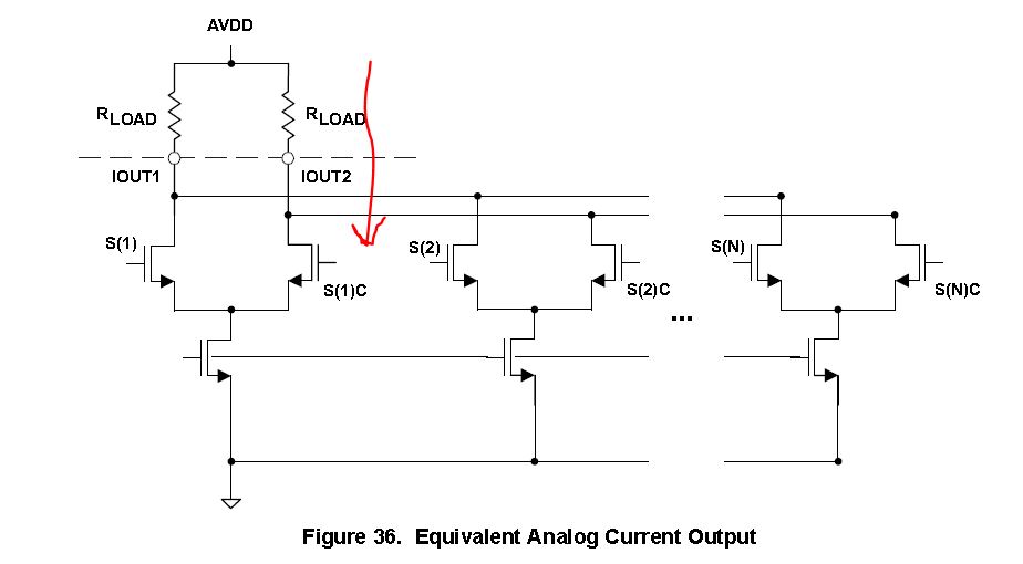
There is an explanation about output compliance range in DAC5681Z as below.

>>The lower limit of the output compliance is determined by the CMOS process. Exceeding this limit may result in transistor breakdown, resulting in reduced reliability of the DAC5681Z device. The upper limit of the output compliance is determined by the load resistors and full-scale output current. Exceeding the upper limit adversely affects distortion performance and integral nonlinearity.

1) I think above AVDD+0.5V, distortion reason is to work ESD diode. Is my understanding correct?

2) I couldn't imagine why AVDD-0.5V may result in transistor breakdown. Could you give me some explanation why this happens?

Best regards,

Toshihiro Watanabe

  • Hi Toshihiro,

    1. Yes your understanding is correct.

    2. As shown is picture below if you output voltage gets below AVDD-0.5V current following through the transistors will also increase due to increase in voltage difference and this increased current may result in transistor breakdown.

    Regards,

    Neeraj Gill

  • Hello Gill,

    Thank you for your answer. I could understood current is contributed for break down, not voltage.

    One question is it seems there is constant current source transistor under S(1) and S(1)C. If under AVDD-0.5V, this transistor can't work as current source anymore so this current flow increases. Could I think correctly?

    Best regards,

    Toshihiro Watanabe

  • Hi Toshihiro,

    We want to operate the N-type MOSFET shown in picture below in Saturation region. The Vgs and Vds are bias such that the transistor remains in Saturation region but  when you violate the lower limit of compliance voltage AVDD-0.5V you are lowering the drain voltage and a result might push the MOSFET to operate in linear region and as result the transistor might not behave switch and as result you might see distortion on the output the DAC.

    Regards,

    Neeraj Gill

  • Hello Gill,

    I understood your answer but one confusion comes up.

    >>The lower limit of the output compliance is determined by the CMOS process. Exceeding this limit may result in transistor breakdown, resulting in reduced reliability of the DAC5681Z device

    Above is written in DAC5681Z datasheet. This says DAC5681Z may break down if output voltage is below AVDD-0.5V.

    From your answer, output may have distortion if output voltage is below AVDD-0.5V because transistor goes into linear region.

    Do we think no problem as below?

    1) Between AVDD-0.5V and GND-0.5V, it may happen distortion.

    2) Below GND-0.5V, device may be damaged due to exeed absolute max.

    I want to confirm if device may be damaged in GND-0.5V ~ AVDD-0.5V region.

    If damaged, please give me some explanation of the reason. I think increasing current won't be happen because linear region or current source existance.

    Best regards,

    Toshihiro Watanabe