This thread has been locked.

If you have a related question, please click the "Ask a related question" button in the top right corner. The newly created question will be automatically linked to this question.

Multiple channel ADC conversion ADS8860 with single voltage reference

Other Parts Discussed in Thread: ADS8860, THS4281, OPA333, ADS8920B, ADS8910B, ADS8881, TINA-TI, OPA625, ADS9110, OPA378

Hello everyone,

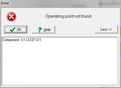
I'm designing a three channel ADC conversion using the ADS8860 at a 1MSPS. I would like to use only one reference voltage for all three channels with the REF5045 and the proposed circuitry of the datasheet with the OPA333 and THS4281. I'm designing the output buffer capacitor (C_BUF_FLT), so that the reference voltage stays within 1 LSB error at the start of each conversion. For that I'm considering the reference input current of all three channels, that is,  Iref=3 x 300 uA, and a maximal conversion time of Tcon_max=710 us. For a 16 bits conversion with 4.5V, results in a 10uF output capacitor (ESR=220 mOhm). My question here is, should this output capacitor be enough to stay within the 1LSB voltage error? or is there something else I should consider in the design when using multiple ADC converters with the same voltage reference? perhaps a 100nF capacitors  at the REF-PIN to decouple the high frequency currents produced by the ADC reference input? 

I would appreciate yours thoughts on this.

Thank you

  • Hi Sebastian,

    We will look into this for you.   Could you please let us know a few more details about your application needs:

    - Please let us know the end application for your circuit; and/or what type of sensor or signal is being measured?

    - What is the maximum sampling rate required in this application?

    - Do you require to sample single-ended signals or differential signals?

    I also would like to mention, we offer the ADS8920B (16-B) and ADS8910B (18-B) devices.  These are differential input, 1-MSPS SAR ADC devices that incorporate the internal reference buffer built into the device, which would simplify the design considerably; as it only require the REF50xx external reference and bypass capacitors for each device.

    Please find a link to the ADS8920B product page below.

    www.ti.com/.../ADS8910B

    Thanks and Kind Regards,

    Luis


  • Hello Luis, 

    Thank you for your answer. Regarding your questions:

    Luis Chioye said:

    - Please let us know the end application for your circuit; and/or what type of sensor or signal is being measured?

    The circuit is for the ADC conversion of current signals in a power converter. Besides the 50Hz fundamental, the currents have high frequency components in the order of tens of kilohertz. The analog signals are provided by a LEM transducer.

    Luis Chioye said:

    - What is the maximum sampling rate required in this application?

    The ADCs are required to work with a sample rate of 1MSPS.

    Luis Chioye said:

    - Do you require to sample single-ended signals or differential signals?

    The analog signals are single-ended. 

    I would take a look at the ADS8920. Nevertheless, I would like to know if it is possible to use the same reference voltage for all three ADS8860s, especially because of the current spikes at the REF-PIN. I might not be able to change to the ADS8920.

    Thanks and kind regards

  • Hi Sebastian,

    Performing a quick calculation, assuming the ADS8860 (16B resolution) device is used in the application, it may be feasible to drive all three ADCs using one REF5045 voltage reference and one composite buffer (OPA333+THS4281) and stay within 1LSB of 16 bit resolution. 

    The SAR ADC reference input pin presents several fast current transients during the conversion period, therefore, it is sensitive to PCB trace inductance.  One suggestion that comes to mind would be to connect the output of the reference composite buffer (OPA333+THS4281) to a single ~220mOhm series resistor; and place local 3.3uF REF bypass capacitors right next to each ADS8860 Reference input pin.  In order to reduce inductance, consider using a copper plane on the top layer for the Reference input pin connections. I would need to set up a couple of simulations to confirm if the Reference droop error is indeed less than 1 LSB of the ADS8860 16B resolution.  It is also important to highlight, the ADS8881 (18B) version has a much smaller LSB size; therefore this approach may not work for the 18B version (ADS8881)  without modifying the circuit.


    Thank you and Kind Regards,

    Luis

  • Hi Luis,

    I appreciate your response. Your proposal with the 3.3uF sounds good. I would appreciate if you could confirm this with your simulations. I tried to do a simulation in TINA-TI with the model of the ADS8860 and setting up the voltage reference with the REF5045+OPA333+THS4281. For a single channel, the simulation works properly, but when trying two or three channels, the simulation does not work.

    I'm only intending to use a 16 bit ADC with the 4.5V reference voltage, so the size of the capacitor should be all right to keep the voltage droop smaller than 1LSB.

    I also looked at the ADS8920. Unfortunately, in my design I'm not able to program the ADC through the SDI pin. Further, since I'll be doing the SMD soldering by hand, the VQFN package would make this task more difficult.

    Thank you once again and I will be waiting for your feedback.

    Kind regards,

    Sebastian

  • Hi Sebastian,

    Performed the TINA ADS8860x3 simulation using the REF5045 and OPA333+THS4281 composite amplifier; and confirmed as well, the droop error is approximately ~2-3LSBs.

    Attached is a different simulation using another composite buffer circuit:  OPA378+OPA625.   This circuit was taken from the ADS9110 datasheet (18B, 2MSPS, SAR ADC).  Each ADS8860 Reference input will require a local 10uF capacitor.  On the TINA simulation, I used 7.1uF capacitors to model the 10uF X7R capacitors, since 7.1uF is the effective capacitance of 10uF 0603 10V X7R capacitors at 4.5V.  Simulation shows the reference droop of  this circuit will be in the order of ~33uV while driving all (3) ADS8860 reference inputs; meeting the 1 LSB requirement for 16 bit resolution.

    Please let us know if you would like us to review the PCB board layout.

    Thank you and Best Regards,

    Luis 

    TINA Simulation:

    ADS8860_simulation_try2.TSC

  • Hi Luis,

    That looks great. That would keep the error to about 1/2 LSB.

    I tried to simulate (menu Analysis\Transient...) the file you sent, but unfortunately I get  the following error:

    In menu 'Analysis\ Set Analysis Parameters' I loaded the 'TINA default' setting and I also tried to increase the 'DC max. iteration number' to '10 000' but I still get the same error.

    Do you know what it could be? Do you use the same settings in TINA-TI? These are my settings in menu 'Analysis\Options':

    It would be great if I could also simulate the circuit.

    Regarding the PCB layout, we are still working on the circuit design. I would appreciate if you could also take a look at the layout. I might contact you about this sometime next week.

    Thank you once again for your help.

    Kind regards,

    Sebastian

  • Hi Sebastian,

    I used the full-version of TINA Classic; where the convergence issue does not appear to occur.  While performing the simulation with the TINA Basic version; I obtain the same error; it may be that the basic version has trouble converging with the complex circuit.

    Attached is a new simulation using a simplified model for the Ref Input of the ADS8860.  The simplified model (developed by colleague Tim Green) is a conservative approximation, as it assumes the worst case where the Reference pin is sampled by the MSB capacitor several times during the 710nS conversion period (the reference is sampled by a binary weighted capacitor for every bit decision during the conversion period).  The conservative result approximates the ADS8860 TINA model on the web but converges much quickly.  The droop on this simulation is around ~47uV, still within ~1LSB 16 Bit requirement for VREF=4.5V 

    Please find attached.

    Thank you and Best Regards,

    Luis

    4527.Simplified SAR ADC REF Pin Model_TG.pdf

    Simulation File: 

    ADS8860x3_simplified_comp_REF.TSC