Hello,
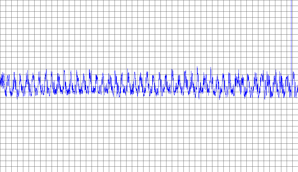
We're experiencing an issue with the Channel 3 output (V1, WCT) on the ADS1293 showing a distortion of the signals. Leads I and II from CH1, CH2 are working fine, but we're seeing the below distortion on Channel 3. This is with a test input 10Hz sine wave on inputs IN1...3, 5. CH1, CH2 show normal sine waves. 
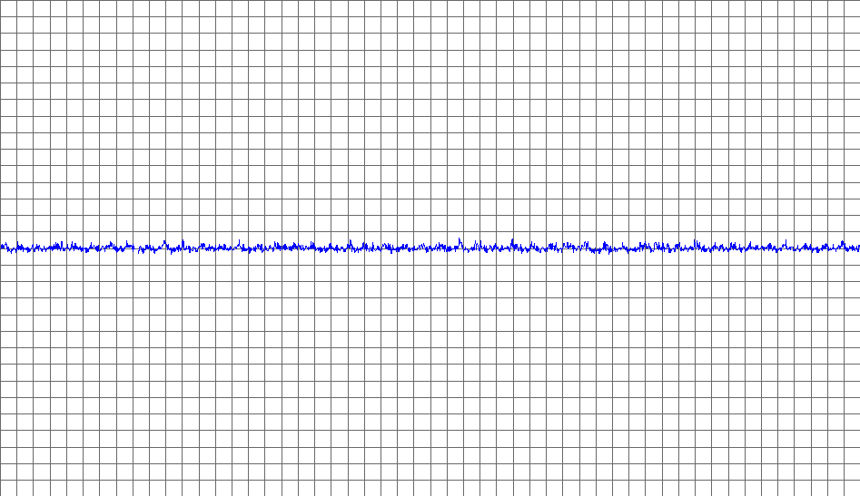
If we short all inputs, CH1 and CH2 are zeroed out but we see this on CH3.
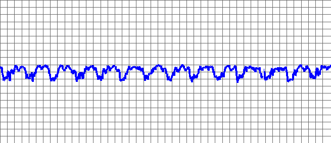
So the distortion in the first screenshot is the sine + interfering signal in the second. Those pulses appear to show roughly every 4.5Hz on the distorted signal. We are using the reference firmware taken in the heartrate example, no modification was done to the register settings as we used the Flash Programmer to directly program the board with the hex file from the project to evaluate the chip. But below are the register settings for the ADS1293 taken from the project. Any idea on what could be causing this?
#define TI_ADS1293_CONFIG_REG_VALUE                         (0x00)                  /* Main Configuration */

#define TI_ADS1293_FLEX_CH1_CN_REG_VALUE                    (0x11)                  /* Flex Routing Swich Control for Channel 1 */
#define TI_ADS1293_FLEX_CH2_CN_REG_VALUE                    (0x19)                  /* Flex Routing Swich Control for Channel 2 */
#define TI_ADS1293_FLEX_CH3_CN_REG_VALUE                    (0x35)                  /* Flex Routing Swich Control for Channel 3 */
#define TI_ADS1293_FLEX_PACE_CN_REG_VALUE                   (0x00)                  /* Flex Routing Swich Control for Pace Channel */
#define TI_ADS1293_FLEX_VBAT_CN_REG_VALUE                   (0x00)                  /* Flex Routing Swich Control for Battery Monitoriing */

#define TI_ADS1293_LOD_CN_REG_VALUE                         (0x00)                  /* Lead Off Detect Control */
#define TI_ADS1293_LOD_EN_REG_VALUE                         (0x7F)                  /* Lead Off Detect Enable */
#define TI_ADS1293_LOD_CURRENT_REG_VALUE                    (0xFF)                  /* Lead Off Detect Current */
#define TI_ADS1293_LOD_AC_CN_REG_VALUE                      (0x00)                  /* AC Lead Off Detect Current */

#define TI_ADS1293_CMDET_EN_REG_VALUE                       (0x07)                  /* Common Mode Detect Enable */
#define TI_ADS1293_CMDET_CN_REG_VALUE                       (0x00)                  /* Commond Mode Detect Control */
#define TI_ADS1293_RLD_CN_REG_VALUE                         (0x04)                  /* Right Leg Drive Control */

#define TI_ADS1293_WILSON_EN1_REG_VALUE                     (0x01)                  /* Wilson Reference Input one Selection */
#define TI_ADS1293_WILSON_EN2_REG_VALUE                     (0x02)                  /* Wilson Reference Input two Selection */
#define TI_ADS1293_WILSON_EN3_REG_VALUE                     (0x03)                  /* Wilson Reference Input three Selection */
#define TI_ADS1293_WILSON_CN_REG_VALUE                      (0x01)                  /* Wilson Reference Input Control */

#define TI_ADS1293_REF_CN_REG_VALUE                         (0x00)                  /* Internal Reference Voltage Control */

#define TI_ADS1293_OSC_CN_REG_VALUE                         (0x04)                  /* Clock Source and Output Clock Control */

#define TI_ADS1293_AFE_RES_REG_VALUE                        (0x00)                  /* Analog Front-End Frequency and Resolution */
#define TI_ADS1293_AFE_SHDN_CN_REG_VALUE                    (0x00)                  /* Analog Front-End Shutdown Control */
#define TI_ADS1293_AFE_FAULT_CN_REG_VALUE                   (0x00)                  /* Analog Front-End Fault Detection Control */
#define TI_ADS1293_AFE_DITHER_EN_REG_VALUE                  (0x00)                  /* Enable Dithering in Signma-Delta */
#define TI_ADS1293_AFE_PACE_CN_REG_VALUE                    (0x05)                  /* Analog Pace Channel Output Routing Control */

#define TI_ADS1293_R2_RATE_REG_VALUE                        (0x02)                  /* R2 Decimation Rate */
#define TI_ADS1293_R3_RATE1_REG_VALUE                       (0x20)                  /* vishy:R3 Decimation Rate for Channel 1 */
#define TI_ADS1293_R3_RATE2_REG_VALUE                       (0x20)                  /* R3 Decimation Rate for Channel 2 */
#define TI_ADS1293_R3_RATE3_REG_VALUE                       (0x20)                  /* R3 Decimation Rate for Channel 3 */
#define TI_ADS1293_P_DRATE_REG_VALUE                        (0x00)                  /* 2x Pace Data Rate for all channels */
#define TI_ADS1293_DIS_EFILTER_REG_VALUE                    (0x00)                  /* ECG Filters Disabled */
#define TI_ADS1293_DRDYB_SRC_REG_VALUE                      (0x08)                  /* Data Ready Pin Source */
#define TI_ADS1293_SYNCOUTB_SRC_REG_VALUE                   (0x00)                  /* Sync Out Pin Source */
#define TI_ADS1293_MASK_DRDYB_REG_VALUE                     (0x00)                  /* Optional Mask Control for DRDYB Output */
#define TI_ADS1293_MASK_ERR_REG_VALUE                       (0xF0)                  /* Mask Error on ALARMB Pin */

#define TI_ADS1293_ALARM_FILTER_REG_VALUE                   (0x33)                  /* Digital Filter for Analog Alarm Signals */
#define TI_ADS1293_CH_CNFG_REG_VALUE                        (0x70)                  /* vishy: 3channels, no status */