This thread has been locked.

If you have a related question, please click the "Ask a related question" button in the top right corner. The newly created question will be automatically linked to this question.

ADC32RF45 TESTMODE

Other Parts Discussed in Thread: ADC32RF45

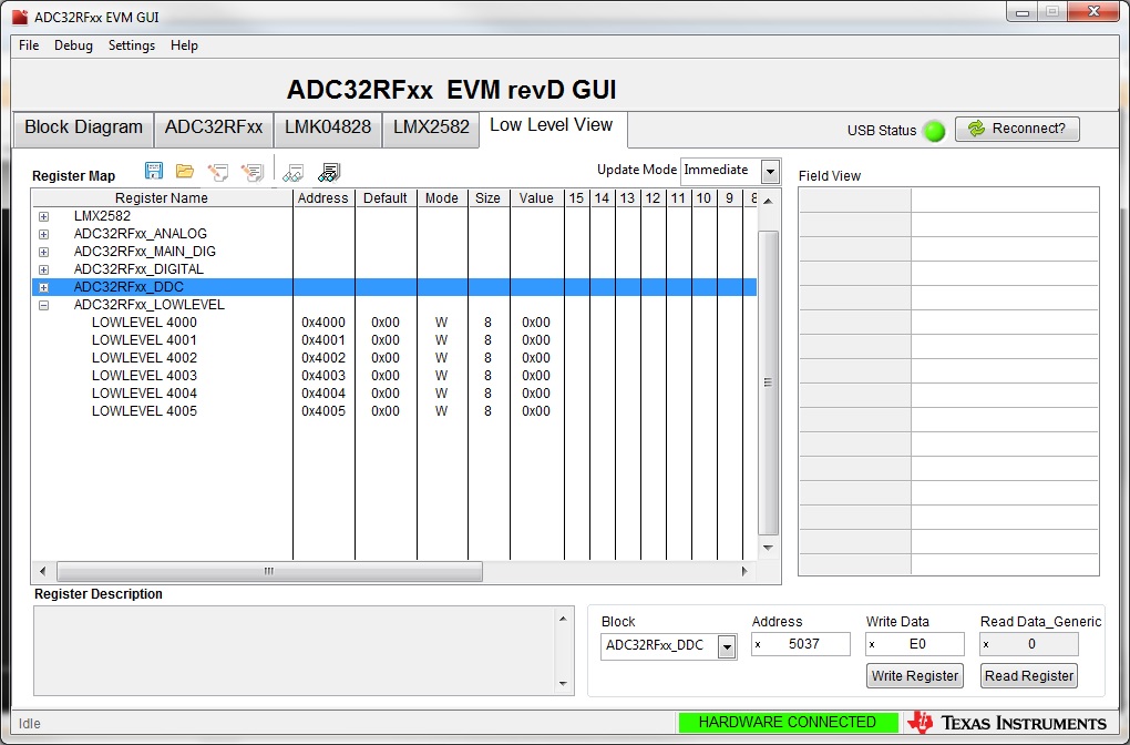
We have the ADC32RF45 EVM and the associated EVM GUI.  So far, I have not been able to get the JESD204B link established.  The ADC datasheet discusses the TESTMODE, controlled through register 0037h.  The GUI does not present this register in the known list, so I have used the raw read/write functions in the LOW LEVEL page.

All reads from that register (and every other "non-listed") register return 00h.  All attempts to write to the register are accepted by the tool (i.e. no error message) but have no apparent effect on the ADC.

Does the raw mode allow read/write of "non-listed" registers?  If so, why doesn't the value I wrote show up when I try to read it back?

Note, I have verified that the ADC is getting its clocks.

Thanks,
Mark

  • Hi,

    Yes, you may use the low level tab to do individual writes to specific addresses that do not have a high level control on one of the higher level tabs.  There are two possible cases involving such a low level access.  In some cases, the register field may have already been described to the SPI GUI in an entry in a spreadsheet even though the field may not yet have a control attached to it yet, and in this case you could just find the address in the list of registers in the middle of the low level tab and then pick and choose bits in that register to set or clear and the definition of that portion of the address should display the name of the field you want to write to.  in other cases the register field may not have been known yet at the time the SPI GUI was created so it would not be already pre-defined, and in this case you would write to the address using the lower right corner of the low level tab, setting the block name, address, data, and clicking Write Register.     The thing to be careful of in using this approach is if the register you want to write to is in a paged address space.  if it is, you would have to use the low level block definition to write all the page addresses first, and then the address within that page.   For example, you might write page address x11 to be 0, page address x12 to be 0, page address x4003 to be 0, page address x4004 to be x69, and *then* write to a register in the JESD digital page.   Since I think the register you are looking for is in the decimation filter page address 0x037 (TEST PATTERN SEL) which is not paged, you might first set all the page addresses to 0, then access this register with address 5037 or 5837 for channels A or B respectively.     So if you do get the access correct for this address then you should be able to read back what was written as well.   Try clearing other page registers to 0 first just to be sure they aren't influencing what register you are accessing, then write something to 0x5037.  If your click on the Read Register button then the GUI knows to set the read bit of the address already turning the address into xD037 so you don't need to worry about that.   Make sure the SYSREF is running as well as the device clock to the ADC also.

    The reason I point out that some register fields may not have a control but still be listed in the register definitions shown in the middle of the low level tab, or not listed at all, is that if you try to write to a register that is not pre-listed in the GUI definitions then you might see that register write flagged as an 'error' or a 'warning' in the log of what register writes have been done, but that is just a warning that the SPI GUI doesn't know what is out there at that register you are writing to.  The register write would still happen, but the SPI GUI doesn't know what that register address is.  (I am talking about the very lower left pane of the window where the SPI actions scroll through as they are performed.  if you double click on that pane you get a popup log window of everything the SPI GUI has done up to that point.)

    Regards,

    Richard P.

  • HI Richard.  Thanks for the many details.

    I am using the lower right corner controls from the Low Level View since the TEST PATTERN SEL register is not included in the register map spreadsheet.

    I think I have followed your advice accurately -- first triggering SYSREF, then writing x00 to addresses x11, x12, x4003, x4004.  (The latter two registers I can confirm since they are in the spreadsheet and I can see them change.)  

    One clarification please.  While trying your advice, I did discover that I must have the correct Block selected as well as typing in the address.  If the wrong block is selected, then the register at the address I think I am accessing will not change.  (I tested this by observing the effect on x4003 and x4004.)  So, which "Block" should I choose when writing to x11 and x12?  

    Nonetheless, I still do not seem to be able to write/read from the TEST PATTERN SEL register.  Screen shot below is register 0x5037 after writing xE0 and then attempting to read it back.

    Thanks,
    Mark

  • I have studied the ADC32RF45 data sheet and programming/register information. The instructions in the datasheet about when and which page registers to use is not very clear. In addition, the registers in the 40__h range are not described in the registers section of the datasheet. Besides 4003h and 4004h mentioned frequently, there appears to be a register 4002h mentioned in sections 8.4.2.3 - 8.4.2.5.

    Is there an update to the datasheet in work to clarify this? Or an app note?