This thread has been locked.

If you have a related question, please click the "Ask a related question" button in the top right corner. The newly created question will be automatically linked to this question.

Data not correct in ADC12J4000EVM Test Pattern mode

Other Parts Discussed in Thread: ADC12J4000EVM, ADC12J4000, LMK04828

Hi everyone,

I built a FPGA project for ADC12J4000EVM.

I configured the board through ADC12J4000EVM GUI.

On the ADC side, the configurations are as follows.

On-board Fs=3760Msps.

Bypass Mode; DDR

L = 8

K = 10

Scrambler off

On the FPGA side, the JESD configurations are as follows.

Refclk = 188MHz

Coreclk = 94MHz

L = 8

M = 10

F = 2

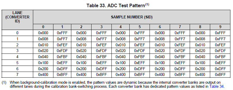
According to page 48 of ADC12J4000 datasheet, the ADC test pattern should be as follows.

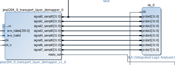
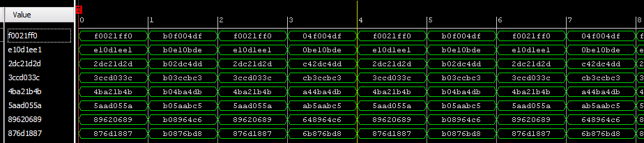
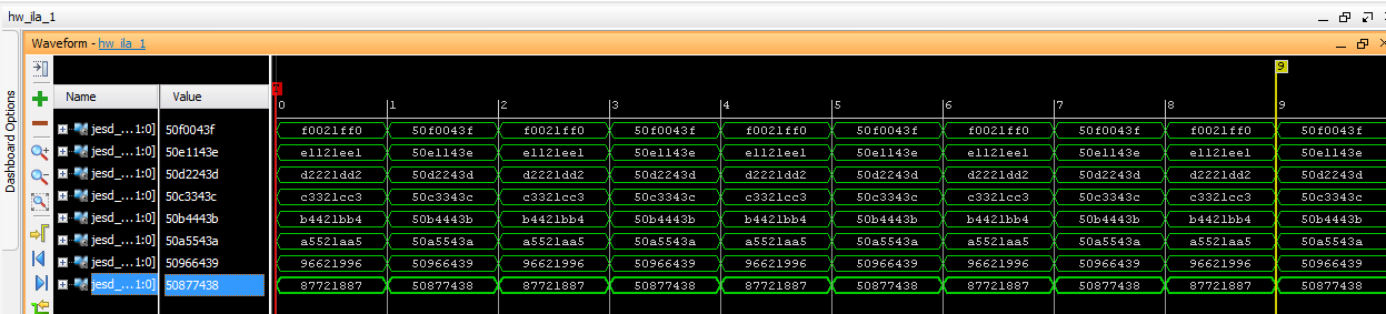
I tried the Test Pattern mode, and exported the data of 8 lanes through ILA. As follows.

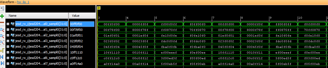
The data from lane 0~2 are the same as the sampled data, while the data from lane 3~7 are not.

Can anyone tell me what I was doing wrong?

Thank you.

Regards,

Tong

  • Hi Tong

    I'm not sure what the problem is. I do have a question about your settings. In your FPGA configuration above, I think the parameters should be as follows:

    L=8, F=8, K=10.

    Did you mean to type M=10 or K=10?

    The product of K * F must equal that of the ADC, which is 10 * 8 = 80.

    To gather more information, can you also configure the ADC EVM into Long/Short Transport Test Pattern mode, and gather a similar data capture?

    The data should match that shown in Table 37 of the datasheet. If it also has differences it may give us a better idea about the nature of the problem.

    Best regards,

    Jim B

  • Hi Jim,

    Sorry I typed M by mistake. I mean K =10.

    The configuration of FPGA was L=8, F=2, K=10.

    In the ADC12J4000EVM GUI, I configured K = 10. But I can't find the option to configure the value of F.

    I have tried to configure FPGA to L=8, F=8, K=10, then I won't receive data from JESD block, since the JESD rdata never became valid.

    The block design in Vivado is shown as follows.

    As it shown in the figure above, the data width of each JESD lane is 32-bit.

    If I configured the ADC EVM into Long/Short Transport Test Pattern mode, the received data will be as follows.

    The data are different from table 37.

    Thank you.

    Regards,

    Tong

  • Hi Tong

    I'm still not sure what the issue might be.

    I do have one thing for you to check. The ADC12J4000EVM that you are using has the P and N swapped in the JESD204B data pairs. This was done to improve the routing and avoid having the cross the P and N lines in between the ADC and FMC connector, and is noted in the board schematics on the FMC connector page. You will need to compensate for this polarity inversion in your receive IP in order to receive the correct data. Since some of the data in your ADC Test Pattern capture looked OK I didn't think this would be the problem, but I may have been wrong. Please confirm you are inverting the lane polarity for all lanes.

    Best regards,

    Jim B

  • Hi Jim,

    I read the schematic of ADC12J4000EVM, the P and N are swapped in JESD serial lanes.

    I didn't noticed this before, since I finished the pin assignment according to TI's reference design.

    Shall I do this by simply adding inverters for the JESD lanes in my FPGA design?

    Is is possible that this problem is caused by the JESD clocks? Is the JESD clock configuration in my design correct?

    Thank you.

    Regards,
    Tong
  • Hi Tong

    I think there is a way to define or change the polarity in the configuration of the JESD204B or the high speed transceiver configuration. You shouldn't add inverters. Your FPGA support folks should be able to give you more guidance on this topic.

    I don't think the problems will be caused by the JESD204B clocking configuration. If the link is staying up consistently then I don't think there can be any clocking problem.

    Let us know how the results look after compensating for the lane polarity inversion.

    Best regards,

    Jim B

  • Hi Jim,

    Thank you very much.

    I'll try to find the method to do polarity inversion.

    The FPGA chip I used is Virtex 7 690t, which belongs to the same family with the chip on TI's VC707 board. There is a TI JESD reference design which interfaced VC707 and ADC/DAC board. But in TI's JESD reference design, I didn't find any configuration of polarity inversion. Could you tell me how did you do the lane polarity inversion in this reference design?

    Another thing is that all my test were finished under the configuration that L=8, F=2, K=10 in the FPGA side. But you have told me the configuration should be L=8, F=8, K=10. However, if I configure the FPGA using L=8, F=8, K=10, the FPGA board will not receive any data from the ADC. Could you tell me if this is a problem?

    Thank you.

    Regards,

    Tong

  • Hi Tong

    In our reference design the polarity inversion is done via configuration settings. The firmware is used in conjunction with an .ini file which includes a parameter to enable the polarity inversion if needed. Here is the file for the VC707 and DDC Bypass mode:

    /cfs-file/__key/communityserver-discussions-components-files/73/0412.ADC12J4000_5F00_BYPASS.ini

    The HSDC Pro software parses this .ini file and configures the firmware accordingly.

    The product of K*F should be the same for both the ADC and FPGA board. F is fixed for each decimation mode. For DDC Bypass mode the F value is always 8 octets per frame.

    With an ADC K value of 10, K*F = 10*8 = 80. The SYSREF signal sent to the FPGA to align the LMFC should be at Fbit/(10*K*F) = 3760*2 / (10*10*8) = 9.4 MHz for DDC Bypass Mode at Fs=3760 MSPS. The default EVM settings will give SYSREF = 23.5 MHz (K=4). Have you updated the LMK04828 divider settings to change the SYSREF frequency to 9.4 MHz?

    The FPGA may also work with K values that give 9.4 MHz as a subharmonic of the calculated LMFC frequency. Other settings will probably be unpredictable.

    I recommend starting with the default K value setting of 4 on both the ADC and FPGA and getting success there before changing to 10.

    Best regards,

    Jim B

  • Hi Jim,

    Thank you very much.

    I figured out how to do the polarity inversion for JESD in Vivado. The polarity inversion could be done by simply tie the pin gtN_rxpolarity_in of JESD to '1'.

    After I configured the polarity inversion and configured the JESD in FPGA side to be L=8, F=8, K=4. The received data are both correct in ADC Test Pattern and JESD short transport test.

    ADC Test Pattern:

    JESD short transport test:

    Regards,

    Tong