This thread has been locked.

If you have a related question, please click the "Ask a related question" button in the top right corner. The newly created question will be automatically linked to this question.

DAC7562-Q1 / output state under the condition of AVDD=0~0.7V

Guru 29720 points
Other Parts Discussed in Thread: DAC7562-Q1

Hi Team,

I understood AVDD must be below 0.7V for at least 1ms, and then be increased up to 2.7V(min) to ensure POR.
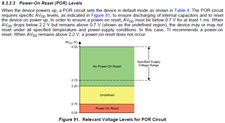


Could you tell me a state of output voltages of DACs under the condition of AVDD=0~0.7V for DAC7562-Q1?
Does these also show zero volts ?

Best Regards,
Yaita / Japan disty

  • Yaita-san,

    During power up an amplifier can often exhibit power-on glitch conditions unless very specific circuitry is implemented inside the device that reduces this power on glitch (or the designer was otherwise aware of and designed to minimize these effects). One of the factors that usually bears strong influence on the magnitude of this power-on glitch is the rate with which the power supply ramps.

    The POR will reset a number of things inside of the device when AVDD crosses the 2.7V threshold, among the actions taken is setting the DAC data register to the default value. There is no static memory inside of the device, though, so at power up the DAC data register should contain 0s assuming the device had been "off" for some period of time, otherwise it may be possible that the data is still present. So if this is a "cold-start" situation I think it should be fine, otherwise complying with the POR description you inserted in your post should avoid any problems.

    Depending on the supply ramp rate (and VOUT loading) I believe all that will be observed at the output is a power-on glitch, which could vary in magnitude. Slowing the supply ramp rate, loading the output with some capacitance, or loading the output with some parallel resistance to the intended load can all reduce the power-on glitch.
  • Hi Kevin-san,

    Thank you for your support.
    I understood Power-on Glitch occurs during power-up as figure 35.

    I would like to ask one more question.
    If AVDD isn't supplied, does outputs of DAC show high-impedance? 

    Best Regards,
    Yaita

  • Yaita-san,

    If the device were powered down then the output amplifier is inactive and not trying to source any current, so in theory I would expect the output pin to look relatively high-impedance. The only caveat would be that there are still ESD cells inside of the device on the VOUT pin, basically diodes that clamp to ground and to the supply rail. If both of these rails are floating or at unknown potentials it's hard to say exactly what would happen if some external potential were applied to VOUT.

    If the signal applied to VOUT while the device was un-powered was referred to the same ground as the DAC7562-Q1 and was a positive voltage with respect to that ground, I would anticipate the ESD cell to the positive rail would become forward biased and sort of "back-power" the device through the ESD cell clamping to the positive supply. This case is risky for two reasons; the ESD cell is not intended to flow large DC currents and this has potential to corrupt the POR OTP read which could lead to some surprise behavior.

    If it were a negative voltage on VOUT with respect to the DAC7562-Q1 ground then the device would not be back-powered and therefore the POR OTP read probably wouldn't be corrupted and nothing unexpected would happen at the VOUT pin, except that the negative clamp ESD cell would have the same vulnerability to excessively large DC current.s