This thread has been locked.

If you have a related question, please click the "Ask a related question" button in the top right corner. The newly created question will be automatically linked to this question.

ADS1115 - Zero reading / OS bit won't assert

Other Parts Discussed in Thread: ADS1115, LM2596

Hello, TI E2E community,

I'm working on the development of a high-precision voltmeter/ammeter project.

I selected the ADS1115 chip since it features 16 bits of resolution and also because it was available at some local electronic shops in my city. I also decided that the first stage of my project should be the testing of the ADC.

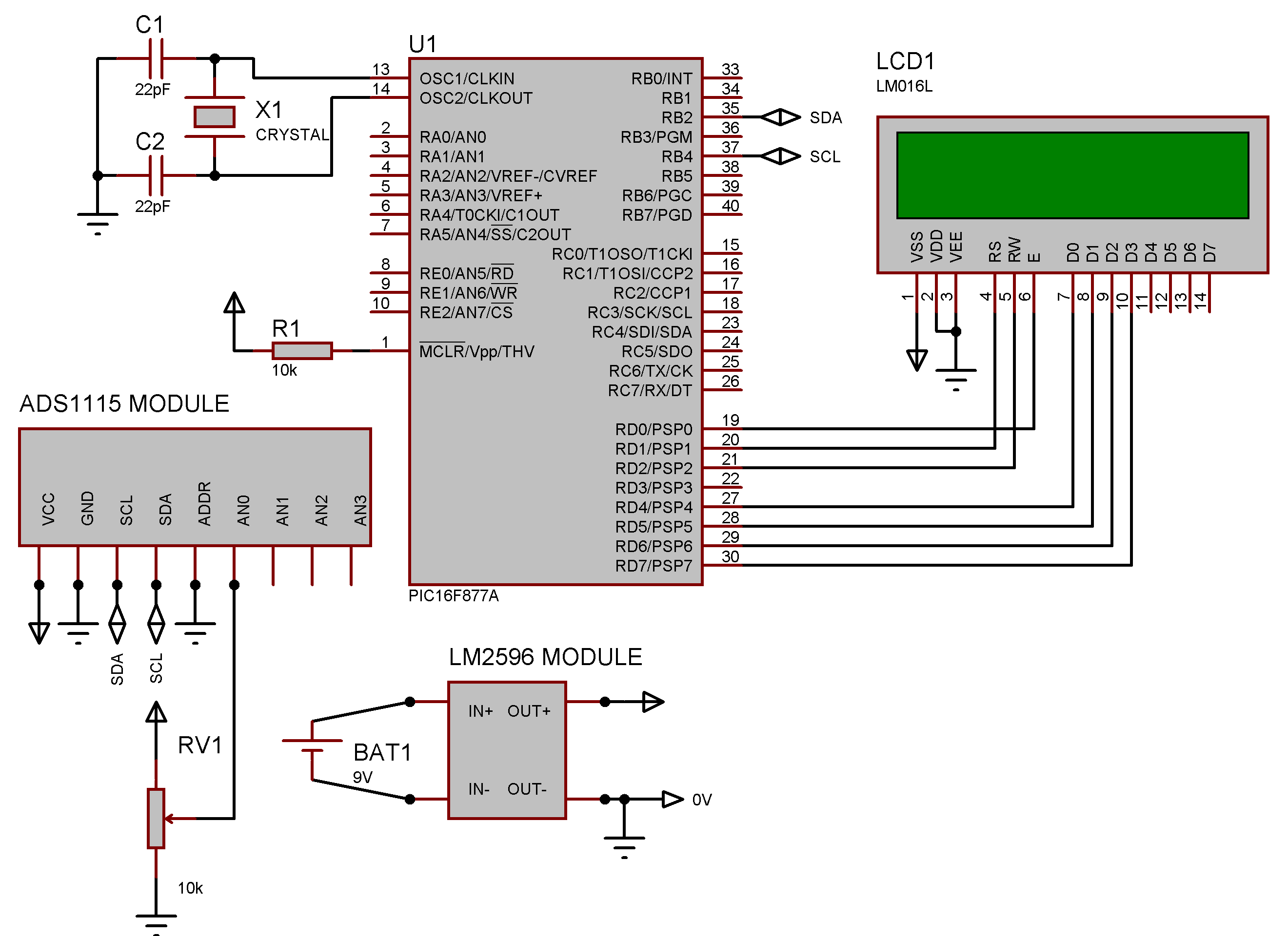
So I bought the ADS1115 module from Adafruit which features the chip itself plus some other components that makes the circuitry implementation even easier. (schematic can be found here: github.com/.../ADS1X15-Breakout-Board-PCBs)

My setup is quite simple. A PIC16F877A communicates with the ADS1115 and 'prints' the readings to a LCD16x2. The ADS1115 chip reads analog voltage from a 10K ohm potentiometer.

The code I'm using in PIC C compiler  is shown below and it contains lines of code with the configuration of the chip:

#include <16f877a.h>
#fuses XT,NOWDT

#use delay(clock=4000000)
#include <lcd.c>

#use i2c(Master,sda=PIN_B2,scl=PIN_B4,FORCE_SW)

void main(){

   int1 flag0;
   int1 flag1;
   int1 flag2;
   int1 flag3;
   int1 flag4;
   int1 flag5;
   int1 flag6;
   
   int msb;
   int lsb;
   
   lcd_init();
   delay_ms(50);
   
   printf(lcd_putc,"\fInicio...");
   delay_ms(1000);
   
   while(1){

      //after a writing, flags go to 0 if master received ACK from slave
      flag0=1;
      flag1=1;
      flag2=1;
      flag3=1;
      flag4=1;
      flag5=1;
      flag6=1;
      
      //-------------------------configuration--------------------------------//
      i2c_start();
      flag0=i2c_write(0b10010000); // address = 0x90 | 0 -> write
      flag1=i2c_write(0b00000001); // 0x01 -> config register
      flag2=i2c_write(0b11000001); // 1 -> os, 100 -> an0-gnd, 000 -> +-6.144 range, 0/1 -> continuous/single conversion
      flag3=i2c_write(0b10000011); // default
      i2c_stop();
      //----------------------------reading-----------------------------------//
      i2c_start();
      flag4=i2c_write(0b10010000); // address = 0x90 | 0 -> write
      flag5=i2c_write(0b00000000); // 0x00/0x01 -> conversion/config register
      i2c_stop();      
      delay_ms(500);
      i2c_start();
      flag6=i2c_write(0b10010001); // address = 0x90 | 1 -> read
      msb = i2c_read();
      lsb = i2c_read(0); // No ACK from master
      i2c_stop();
      //----------------------------output------------------------------------//
      printf(lcd_putc,"\f%u %u %u\n%u %u %u %u",flag0,flag1,flag2,flag3,flag4,flag5,flag6); //makes sure the whole COM process was fine
      delay_ms(1000);
      printf(lcd_putc,"\fmsb,lsb=%u,%u",msb,lsb); //msb and lsb from conversion displays on lcd 16x2
      delay_ms(1000);
      
   }
}

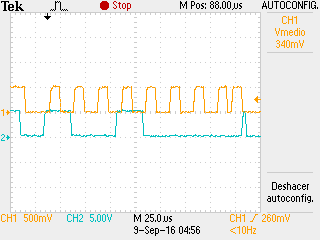
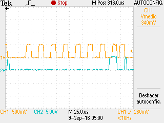
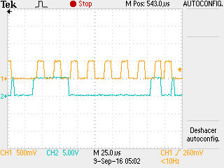
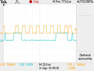
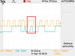
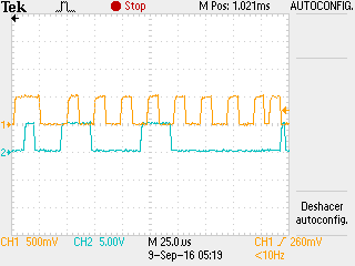
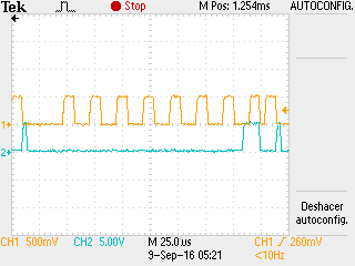
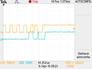
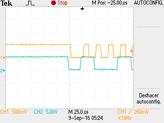
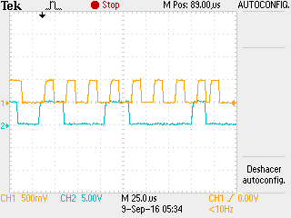
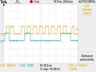
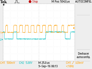
The flags variables are printed as '0's on the LCD, which means that communication is going well and the chip isn't  broken. However the problem is that whenever I read the conversion register, I get msb=0 and lsb=0. And the reason for this is that, when I change the code in order to read the configuration register, I get msb=65(0b01000001) and lsb=131(0b10000011) which means that even after 500ms of delay the conversion is still in progress (OS bit is cleared).

Why is this happening? I guess that timings could not be correct, but I read from other threads that this should not be a problem in power-down mode. I've read the datasheet many times and I can't figure out what could be wrong. I've been working on this issue for many days now and I'm running out of ideas.

Some additional information about my setup:
- I'm powering my entire circuit with the output of a switching converter module (the LM2596 module to be precise) whose input is a 9V battery.
- My circuitry is built on a breadboard.
- The I2C lines are connected by jumpers that are 15cm long at max.
I tried using the actual I2C module from the PIC, which uses RC3 and RC4 pins but for some reason it ends up printing msb=255 and lsb=255 on the LCD. That is why I stuck with the software implementation through normal GPIO pins (B2 and B4).

PD: If anybody knows if it is possible to simulate the chip (ADS1115) in Proteus or some other similar software it would be great if you could post it in this thread because every time I wanted to test my code I had to "burn" my code onto the PIC so that really slowed down the development of my project.

Thanks.

github.com/.../ADS1X15-Breakout-Board-PCBs

  • Hello Marconico,

    We will get back to you shortly.


    Thanks,

    Krunal

  • Marconico,


    I'm the best at looking at code, but it does look like you are able to read and write to the device. However, I would still try to get an oscilloscope just so that you can see the SDA and SCL lines.

    Just to make sure you have the settings that you want, you are measuring from AIN0 to GND, you have the device in power down mode, running the ADC at 128SPS. The comparator is disabled. How do you have the input setup. You mention that you have a potentiometer, but are you using a set current source to make voltage measurement? I would definitely make sure that the input voltage is correct by measuring the voltage back with a multimeter. It might also be helpful to get a schematic of your setup, including the potentiometer and current source.

    Since you're having problems with the power down mode, have you tried using the device in continuous conversion mode instead? I would check to see if you are able to make any measurements at all. You might want to check different gains and data rates to see if you get anything different. If you've damaged the device, you might also want to check different input channels as well.

    Regardless, check into different configurations and see if it helps. Then post back.


    Joseph Wu
  • Thanks for your answer, Joseph.

    As you said, I used an oscilloscope to measure the waveforms of the SDA and SCL lines.

    These are the results when I attempt to read the config register after a conversion:

    1. Start and First byte (write 0b10010000 -> address and write bit)

    2. Second byte (write 0b00000001 -> select config register)

    3. Third byte (write 0b11000001 -> start conversion, read from an0-gnd)

    4. Fourth byte (write 0b10000011 -> default)

    5. Stop and start (inside the red box)

    6. First byte (write 0b10010000 -> address and write bit)

    7. Second byte (write 0b00000001 -> select config register)

    8. Stop, wait 500ms, and Start again


    9. First byte (write 0b10010001 -> address and read)

    10. Second byte (read 0b01000001 -> OS bit is cleared)

    11. Third byte (read 0b10000011 -> default lsb byte from config register)

    Additionally, I tested the same code with an1-gnd, an2-gnd and an3-gnd and the results were the same.

    My schematic of the circuit looks like this:

    I also checked the voltage at the pin (by measuring voltage between the top of the pin welding spot and ground).

    I tried with continuous mode but OS bit stays cleared too.

    I guess that even though the I2C module of the chip is ok, the ADC module could be damaged for some reason I ignore (I've never put voltages out the range of 0-VCC to the ANX pins). What could have happened? Or maybe I overlooked something in the oscilloscope waveforms?

    A couple of days ago I bought another ADS1115 module, and I'll be testing it soon.

    Thanks again for your answer.

    Marco.

  • Marco,


    Before I start, I noticed that I had written my response incorrectly. I should have started with "I'm NOT the best at looking at code...." I generally help with ADCs and how they are used from a circuit perspective. I don't do a lot of coding and therefore, I'm really not great at reading through it.

    Going back to the scope shots, right now it looks like you have:

    Write to device, config register, C1 83
    Then STOP/START
    Write to device, config register, wait 500ms, read from the device, get back 41 83

    I would try to change the timing of the read and treat the 5 byte transaction as a single operation. Instead of what you have, try:

    Write to device, config register, C1 83
    Then STOP, wait 500ms, then START
    Write to device, config register, read from the device, get back two bytes.

    My concern would be that by starting the read and then waiting that the read has already started and that the configuration data is already moved to some output shift register. In this case, you're splitting the read up so that the data comes from before the 500ms delay. This would explain why read back of the OS shows that the part hasn't completed the conversion.


    Joseph Wu
  • First of all, thanks for answering again. I had the feeling that a week old thread wouldn't get another answer (lol).

    Anyhow, I tested the recently purchased ADS1115 module I mentioned in my previous reply and it worked just fine. I'm even programming the chip for the next steps of the project (which is great). So, the first chip was broken from the beginning.

    To make a conclusion to this thread I'll just state the following:

    1. My first code was fine. Joseph, if you notice, actually the 500ms happens between a stop and a start.

    2. The code mentioned could help others to debug the communication between a PIC and the chip.

    3. The reason I think OS bit didn't assert is because the ADC sub-module was somehow damaged but the I2C one was fine.

    Thanks to everybody.

    Marco

  • Marco,


    I'm glad that worked for you. If you have any other questions, feel free to post back.


    Joseph Wu