This thread has been locked.

If you have a related question, please click the "Ask a related question" button in the top right corner. The newly created question will be automatically linked to this question.

Simulation JESD204B for ADC12D1800 in HyperLynx 9.2

Other Parts Discussed in Thread: ADC12D1800

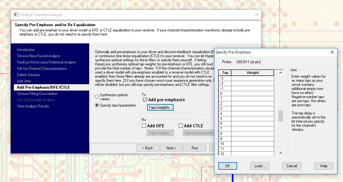
Hello Dears. I'm simulation Digital Section ADC12D1800 in HyperLynx 9.2. I Need to characteristics Equalization this Chip. 

Thanks for Attention.

  • Hi Sina

    The ADC12D1800 uses LVDS for the output data interface, not JESD204B. The maximum possible data rate is 1800 Mbit/sec when operated in Non-Demux Mode. The LVDS outputs on this device only have two adjustable characteristics, as follows:

    1. Output common mode voltage, selected by either letting the VBG pin float, or connecting the VBG pin to the positive supply voltage.
    2. Output differential swing, selected via the OVS control bit.

    The resulting differential output swing and common mode (offset) voltage are described in the Digital Output Pins portion of the datasheet specification table. The VOD and VOS parameters are shown for the different possible combinations of settings.

    The LVDS output behavior is modeled in the IBIS file available here: http://www.ti.com/lit/zip/snam014

    The following portion of the IBIS file defines the 4 different combinations:

    [Model Selector]  lvds_hs
    lvds_lo_vbgf      output voltage=lo, vbg=floating
    lvds_hi_vbgf      output voltage=hi, vbg=floating
    lvds_lo_vbg1      output voltage=lo, vbg=hi
    lvds_hi_vbg1      output voltage=hi, vbg=hi

    Best regards,

    Jim B