This thread has been locked.

If you have a related question, please click the "Ask a related question" button in the top right corner. The newly created question will be automatically linked to this question.

ADC32RF45: Interleaving spurs performance as a function of the sampling rate

Other Parts Discussed in Thread: ADC32RF45, ADC32RF45EVM, LMK04828

Hi everybody,

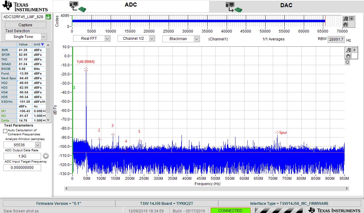
 I have been evaluating the ADC32RF45 for a few days by means of an ADC32RF45EVM + TSW14J56EVM and the original cfg files provided along with the EVM's software.Currently I am configuring the EVM so that I can generate the ADC's sampling clock from an external signal generator, and after many tests, I observed that the ADC's performance in terms of interleaving spurs suppression appears to depend on the selected sampling frequency. For example, the spectrum that I get after digitizing a 666 MHz analog tone is:

1500 MSPS: Not very bad

1600 MSPS: Similar thing

1700 MSPS: Interleaving spurs increase quite dramatically and noise floor appears colored (¿?)

1800 MSPS: Same thing but even worse

1900 MSPS: Good performance back again

This phenomenon was repeatable on all tests that I performed, and it does not depend on the analog input tone's frequency. I mean, I tested many different frequencies between 10 MHz and 800 MHz with the same results: whenever the sampling rate was between 1700 - 1800 MHz, interleaving images suppression decreased significantly. I even tried to vary the frequency of the input tone so that the digital frequency of the sampled signals (i.e. the frequency in rad) was the same on all cases, but again, depending on the sampling rate I got better or worse interleaving spurs suppression. If somebody is interested in seeing the rest of the captures I made -maybe for a comparison- I can upload them, just tell me. There are quite a few.

I would like to know if this phenomenon is normal, or if I could be messing the setup somehow, since the converter's specifications are given for sampling rates of 3GHz (or something like that) on the datasheets. About my setup and setup proceure:

- HW and SW: ADC32RF45EVM rev D + TSW14J56EVM rev B, HSDC Pro v4.2 and ADC32RF45 EVM 2.1, both running on Windows 10.

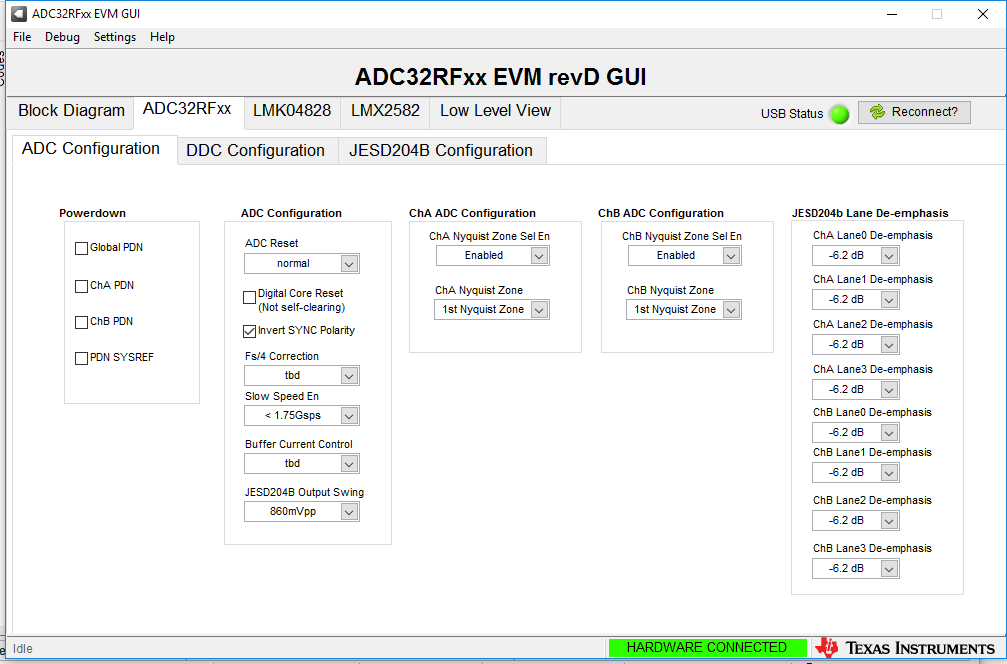
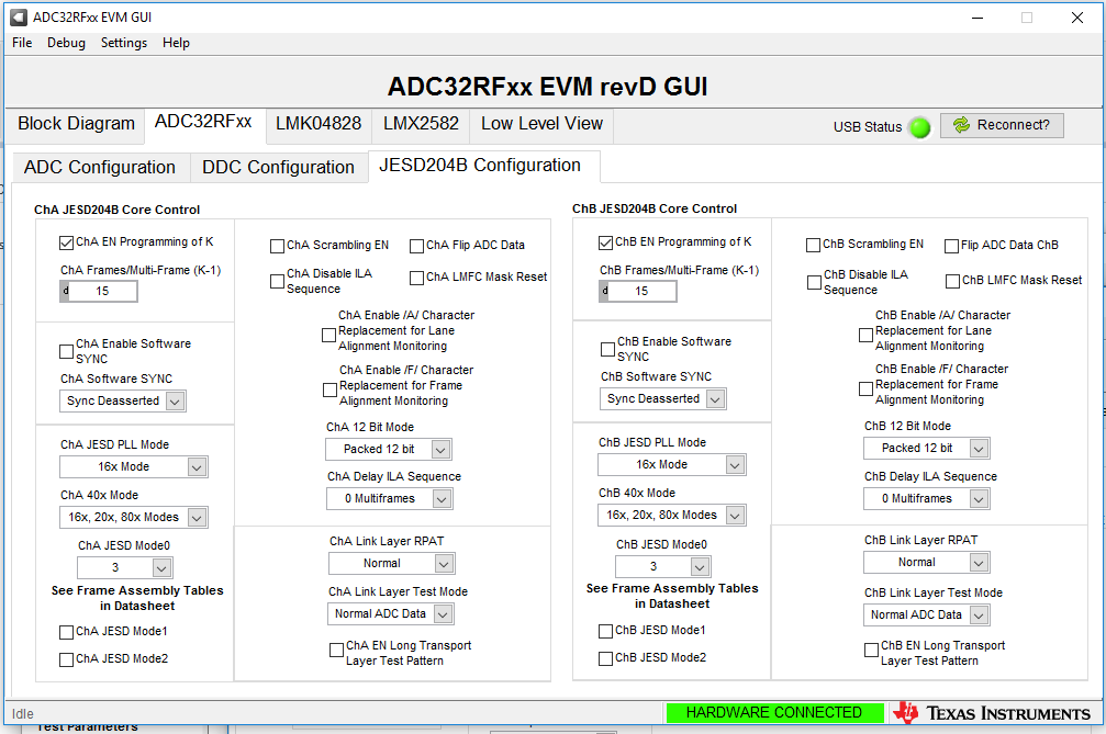
- The EVM is configured as indicated in the ADC32RF45 User Guide. Config files are LMK_ADC32RF45_LMF_82820_ExtClock.cfg and ADC32RF4x_12bit_LMFS_82820.cfg, written in that order after a reset on the LMK, and with an intermediate hard reset on the ADC.

- I'm using a single clock source to provide the ADC's clock and the LMK04828's reference by means of an splitter. The generator is adjusted so that power is about 7dBm at the EVM's SMA connectors. The clock is BP-filtered to suppress any harmonics.

- Power consumption is about 1.3A before configuring the LMK and ADC, and about 1.8A afterwards. Power supply is limitted to 4A and the current limitter stays off all the time.

- The analog signal is synthesized by means of a second signal generator and some BP or LP filters depending on the tests; input power is about 2-3dBm at the SMA connector.

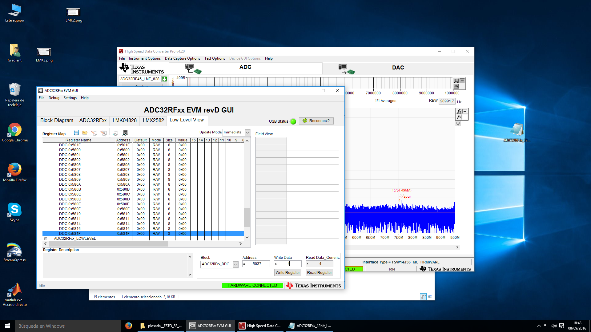
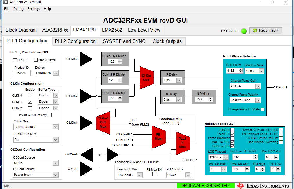
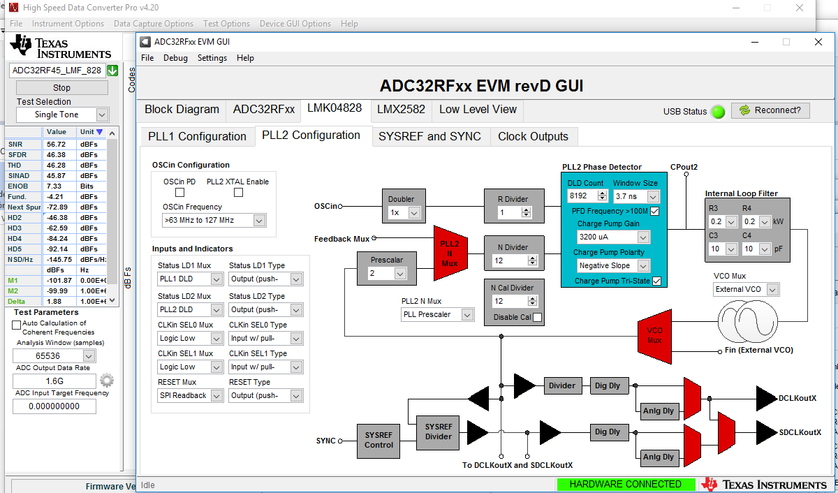
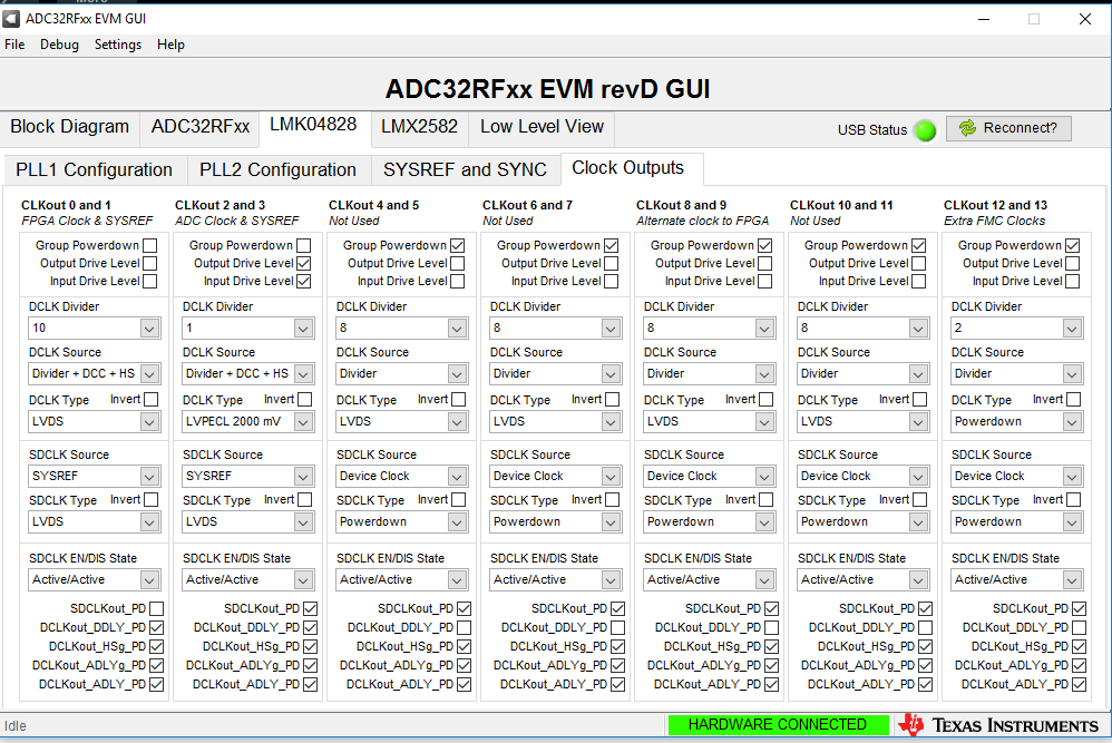
Some captures of the EVM software showing ADC and LMK configuration:

The "Slow speed En" was adjusted depending on the actual sampling rate (< 1.75 GHz for 1600 and 1700 MSPS) with no impact on the results.

LMK04828:

Two more things before I finish:

- I have noticed a strange thing on the TSW14J56EVM: according to the user guide (SLWU086C), LED D3 indicates that the ADC is synchronized with the JESD204B receiver on the FPGA side when it is OFF, but in my case this led stays ON excepting for a few tenths of a second every time I perform a capture. Data appears to be all right, but I do not know if this is a symptom of something not going 100% well. LEDs 2 and 4 blink at a few Hz as indicated on the previous document.

- I have noticed as well the Fs/8 notches of the interleaving correction block (this is explained in this post) when I inject tones at the input. My question is: the "filters" that Mr indicates on the previous post are always there? I mean, if I sample, say, a 6 MHz wide QAM signal centered at Fs/8 for a given Fs, will this filtering effect obliterate my signal?

Anyway, I would really appreciate any information regarding these questions or the issue I have with performance and sampling rates.

Thank you very much in advance and sorry for the long post.

B.R.

Pablo.

  • I forgot to say that the ADC32RF45 and the TSW14J56EVM were both power-cycled and reprogrammed between tests. Once powered up, the sampling clock's frequency was never changed.
  • Hi,

    I will set up an EVM and recreate the captures at the conditions you list, and post what I see.   We have moved on from the TSW14J56 revB capture card to the current revD capture card, but at your sample rates it should not make a difference   The FPGA firmware for the revD capture card has the adaptive EQ of the FPGA enabled which is needed for the full 12+ Gbps line rate of the JESD204b lanes at 3Gsps.   The revB capture card ran out of steam around 10Gbps or so on the serial lanes.   Not a problem down around 2Gsps or so where you are looking.   

    I do note that there are two bits described in the datasheet for the ADC32RF45 for low speed mode, and these bits should be set for sample rates below 1.75Gsps.  The config files you are using do not set these bits.  Curious that you run into trouble right around that area, but that it clears up at sample rates higher *and* lower than that.     But the spectrum you see at 1.8Gsps is not expected. Something is wrong there.  I will have to go see what I get there.    It won't be optimal at 1.8Gsps, as the device is trimmed for operation at 3Gsps but it should be quite functional.

    And yes, the interleaving correction circuitry and filtering will wipe out your signal at Fs/8 and integer multiples of that.  it is expected that the sample rate and/or location of the input signal be chosen to plan around the Fs/8 locations.   By default the interleaving correction is enabled.  It can be disabled, but I am still looking to find out if the interleaving correction logic is an all-or-nothing choice or whether just certain aspects of it can be disabled.

    Regards,

    Richard P.

  • Hi Richard,

    Thank you very much for your prompt response, I would really appreciate that you tried to replicate my captures so we can compare them.

    With regard to the two bits that you mention, I checked them out and they are linked to the "Slow Speed En" control in the middle of the ADC32RF45 Configuration page. Whenever you change this control you can see on the Low Level page that bits SLOW SP EN 1 and 2 in registers 0xD5 and 0xD8, respectively, are modified accordingly. In any case I set them properly for the sampling rate I generated on each test, although I saw that there was no difference at all in the results if I skipped this.

    I have a couple of questions more about the TSW14J56EVM:

    - When I configure the depth of a capture in HSDC Pro to a "large" number of samples, say 10 millions, are those samples taken continuously in time? I mean, does the TSW14J56EVM gather the 10 million samples continuously and then transfers them to HSDC, or they are formed on the HSDC as a succession of shorter, not necessarily continuous, captures?

    - On the other hand, I am unable to enable the test pattern at the digital block level. My intention is to enable this test pattern so that I can capture it directly on HSDC and them export it to Matlab for further inspection (as this would answer my previous question). From what I read on the datasheets, it should suffice with writting register 0x037 at the decimation filter page (according to the datasheets, the decimation page accepts direct addressing), but so far I could see no test patterns at all. What I have done to try to enable it is to write 0x04 to address 0x5037 in the decimation filter page, as depicted below:

    Could you please help me with this?

    Thank you very much and best regards,

    Pablo.

  • Hi,

    while I am still setting up to look at your conditions, let me answer some of your other questions.

    The TSW14J56 revD allows for a capture of as much as 2G samples, which for a  2channel EVM like the ADC32RF45 means as much as 1Gsample per channel.  And the captured data is continuous without any gaps.    The FFT processing is capped at 512K in the GUI ini file so as to not accidentally start something that might take hours to complete on the PC, but the max FFT length can be manually edited in the ini file for instances where you really want to commit to doing a big FFT.    But a 10M capture is not a problem, and it will be continuous data.

    Setting up a test pattern like the arithmetic ramp is easy in the 12bit LMFS=82820 mode as there is just the one DPI bit to enable it.    For the DDC modes, I have been given a short sequence of SPI writes to set up both channels to output a ramp.  It uses addresses x037 and x038, as well as x039 and  toggling a bit at address x03A.    I haven't reconciled this little script with what I see in the datasheet, but I was handed this script and I have used it, and have seen the resulting ramp pattern out.   I have not added these test modes to the SPI GUI yet but I will be.   I saved this into a cfg file of its own that could be loaded after the other cfg files. Please see attached.   ADC32RF4x_DDCmodes_ramp.cfg

    0x5839 0x00  
    0x5837 0x44   // Pattern Code for ChB: all_0=0x11, all_1=0x22, toggle(16h'AAAA/16h'5555)=0x33, Ramp=0x44, custom_single_pattern1=0x66, custom_double_pattern1&2=0x77
    0x5838 0x44   // Pattern Code for ChB: all_0=0x11, all_1=0x22, toggle(16h'AAAA/16h'5555)=0x33, Ramp=0x44, custom_single_pattern1=0x66, custom_double_pattern1&2=0x77
    0x583A 0x00
    0x583A 0x02
    0x583A 0x00
    0x5039 0x00  
    0x5037 0x44   // Pattern Code for ChA: all_0=0x11, all_1=0x22, toggle(16h'AAAA/16h'5555)=0x33, Ramp=0x44, custom_single_pattern1=0x66, custom_double_pattern1&2=0x77
    0x5038 0x44   // Pattern Code for ChA: all_0=0x11, all_1=0x22, toggle(16h'AAAA/16h'5555)=0x33, Ramp=0x44, custom_single_pattern1=0x66, custom_double_pattern1&2=0x77
    0x503A 0x00
    0x503A 0x02
    0x503A 0x00

    Regards,

    Richard P.

  • Hi Richard,

     Thank you very much for the information and for the script. I checked the test pattern and the JESD204B link seems to be working all right on both channels, there are no glitches or missing codes in the ramps. Just a minor detail: as far a I know there is no reference to the DPI bit that you mention in the AD32RF45 datasheets, so I could not enable the test pattern for mode 80820. I loaded the script you attached instead, and what I saw was that each code in the test pattern is actually repeated 16 times (I suppose this is what you end up with when the DDC is disabled). You can see this "stepping" effect on the attached CSV file if you want.

    TestPattern.txt

    With respect to enabling the test pattern at the digital block layer on mode 80820, the only relevant fields I see in the datasheets are explained in pages 80 - 81. There are a couple of reset bits (one self-clearing, another non-self-clearing) and the test pattern selection itself. I tried to set the pattern selection field and then toggle the non-clearing reset (similarly to what's done in your script) but no luck.

    While I was doing some more tests I found something funny though. Under the same conditions and setup procedure listed in my first post, I found out that waveforms sampled by channel B always show high interleaving spurs, regardless of the sampling frequency. So far I have been using channel A only, and I supposed channel B would perform in a similar manner, but it seems that the problem is even worse.

    I made a couple of tests at 1800 MSPS and 1900 MSPS, and channel B's output spectrum looks like this:

    - 1900MSPS, 47 MHz input, 48 MHz AA Filter, -5dBm input power at SMA connector

    - Same signal sampled by channel A

    I could upload similar figures for 1800 MSPS. Again, I did not touch anything on the LMK and ADC cfg files, the power supply's current limiter is off, reference clock power is 7dBm at the SMA, etc.

    Do you have any idea about what could be wrong?

    Thanks for your help.

    P.

  • Hi,

    for the ramp pattern for the LMFS_82820 mode, there is a single bit in the JESD Digital page address x03 called RAMP 12BIT.  Page 69 of the datasheet.   This bit enables that one test pattern to appear in the data for the LMFS_82820 mode. 

    There should be no appreciable difference in the behavior of channel A vs channel B, unless there is a setup issue.  I will look at both channels when I check these sample rates on my bench.

    Regards,

    Richard P.

  • Hi Richard,

     Thanks for the clarification, I had thought that the bit you mention enabled the JESD204B link layer test pattern instead, which I am not sure if I could see from HSDC Pro. I will check that this afternoon.

    I am looking forward to comparing your setup and results with mine. I would really (really) appreciate if you could also indicate the power of your clock signal at the SMA input of the ADC23RF45EVM, and whether you employ two synchronized signal generators or a single one and a splitter to derive the required ADC and LMK clocks. I am running out of ideas to deal with this problem.

    Best regards and thank you again,

    P.

  • Hello Richard,

     Could you perform any measurements?

    Regards,

    P.

  • Hi,

    yes, I did.  And I see the same behavior you do.  I have asked the design team to look into this for me.  I suspect it will be something else that I will have to add to the configuration file, but that is what I am waiting to find out.

    Regards,

    Richard P.

  • Richard,

     Thank you very much for the information, I really appreciate it. I was at the point of thinking that my board could be fried or something, so your reply is quite a relief. If you find out the proper configuration, please consider posting it or updating the EVM software package, we are still interested in seeing how the ADC32RF45 performs at 1800MSPS.

    By the way, I noticed the update of the datasheets but as far as I have seen, no mention to the Fs/8 notches effect and whether they can be disabled or not. Is this going to be detailed somewhere?

    Thank you very much again and BR.

    P.

  • Hi Richard,

     Any news on this problem?

    Best regards,

    P.

  • Hi,

    I have pinged the design team.  I see from the Outlook auto-response that my main contact in the team is out of office, although he has been responsive to email when he can.  and I have copied in another person from the design team, so I will see what I can find out.

    Regards,

    Richard P.

  • Hi,

    The design team looked at those conditions and report that enabling the slow speed mode takes a few more bits to be set than the draft datasheet indicated.  And the lower limit for when the slow speed mode is needed has been raised to 2.5Gsps.   The next datasheet revision will correct this.  Their exact response is below, and I will try this out on my lab bench as well but wanted to get this to you quickest:

    NOTE: Slow mode has to be enabled for speed lower than 2500MSPS.


    There is a discrepancy in the address of slow mode enable mentioned in the datasheet, we have corrected it in the latest revision of datasheet.


    Correction in address mentioned below


    0D5 has to be 03F

    0D8 has to be 042


    Regards,

    Richard P.

  • Hi Richard,

     Thank you very much for the information, I really appreciate your help. I will not have access to the ADC32RF45EVM for a few days, but as soon as I get it back I'll try to enable the slow speed mode and repeat the tests.

    If you try this solution out and get it to work please let me know (I'll have an even better reason to recclaim the EVM).

    Best Regards and thanks again!

    P.