Other Parts Discussed in Thread: ADS1255
Hello!
Currently I am studying ADC ADS1255 using stm32 with chibios. I have developed a prototyping board for the ADC . Board contains the power supplies of analog and digital parts ( 5 V, as the reference 2.5V and 3.3V ). XTAL 8 MHz 10ppm. Scheme is represented below

I have carefully studied the datasheet and wrote a minimally functional program that performs the following tasks:
1) Power up sequence;
2) Reset sequence;
3) ADC configuration;
4) Data receiving.
Here is the code:
// Sending command to ADC
void ads_command(uint8_t command) {
CsLo(); // Chip select low
uint8_t temp = command;
spiSend(SPI_Driver, 1, &temp); // spiSend is chibiOS's function, that send n bytes (1 in this function) from the variable "temp"
CsHi(); // Chip select high
}
// Reset ADC
void ads_reset(void) {
ads_command(ADS125X_RESET);
chThdSleepMilliseconds(MS2ST(4)); // 4 ms delay
ads_command(ADS125X_SELFCAL);
chThdSleepMilliseconds(MS2ST(10)); // 10 ms delay
}
// Wakeup ADC from Standby
void ads_wakeup(void) {
ads_command(ADS125X_WAKEUP);
}
// Write data to ADC's register
void ads_wreg(uint8_t firstreg, uint8_t numreg) {
uint8_t temp = ADS125X_WREG + firstreg;
CsLo();
spiSend(SPI_Driver, 1, &temp);
temp = numreg-1;
spiSend(SPI_Driver, 1, &temp);
spiSend(SPI_Driver, numreg, ®stack); // regstack - is a global array (length 0x0A) for ADC's reg data collection
CsHi();
}
//Read data from ADC's register
void ads_rreg(uint8_t firstreg, uint8_t numreg) {
uint8_t temp = ADS125X_RREG + firstreg;
CsLo();
spiSend(SPI_Driver, 1, &temp);
temp = numreg-1;
spiSend(SPI_Driver, 1, &temp);
chThdSleepMilliseconds(MS2ST(2));
spiReceive(SPI_Driver, numreg, ®stack);
CsHi();
}
void ads_rdatac() {
PWaitingThread = chThdGetSelfX();
chSchGoSleepS(CH_STATE_SUSPENDED);
ads_command(ADS125X_RDATAC);
}
void ads_sdatac() {
PWaitingThread = chThdGetSelfX();
chSchGoSleepS(CH_STATE_SUSPENDED);
ads_command(ADS125X_SDATAC);
}
// Read ADC's conversion data in continuous mode
void read_data(uint8_t numdata, void *pbuff) {
CsLo();
for (uint8_t i=1; i < numdata+1; i++) {
PWaitingThread = chThdGetSelfX(); // Here is a routine that wainting for external event (DRDY changing from high to low)
chSchGoSleepS(CH_STATE_SUSPENDED); // to perform read operation
spiReceive(SPI_Driver, 3, pbuff);
pbuff = pbuff + 3;
}
CsHi();
}
// One shot mode
void read_data_oneshot(uint8_t numdata, void *pbuff) {
ads_sdatac();
for (uint8_t i=1; i < numdata+1; i++) {
PWaitingThread = chThdGetSelfX();
chSchGoSleepS(CH_STATE_SUSPENDED);
ads_command(ADS125X_RDATA);
CsLo();
spiReceive(SPI_Driver, 3, pbuff);
pbuff = pbuff + 3;
CsHi();
}
}
void ads_conf() {
ads_rreg(0,1); // read status
regstack[0] = regstack[0] | ADS125X_BUFON; // Change reg value
ads_wreg(0,1); // Buff on
regstack[0] = 0x01; // Positive - AIN0
ads_wreg(0x01, 1); // Negative - AIN1 differential mode
regstack[0] = 0xB0;
ads_wreg(0x03,1); // Sampling speed 2 kSPS
ads_rreg(0x02,1);
regstack[0] = regstack[0] | 0x00; // PGA = 1
ads_wreg(0x02,1);
ads_command(ADS125X_SELFCAL); // Self calibration
chThdSleepMilliseconds(MS2ST(2));
}
/*
* Threads
*/
int main(void) {
halInit();
chSysInit();
/*
* GPIO configuration
*/
palSetPadMode(GPIOSPI, CS, PAL_MODE_OUTPUT_PUSHPULL); /* CS */
palSetPadMode(GPIOSPI, SCK, PAL_MODE_ALTERNATE(5) | PAL_STM32_OSPEED_HIGHEST |GPIO_MODER_MODER5_1); /* SCK */
palSetPadMode(GPIOSPI, SO, PAL_MODE_ALTERNATE(5) | GPIO_MODER_MODER6_1); /* MISO */
palSetPadMode(GPIOSPI, SI, PAL_MODE_ALTERNATE(5) | PAL_STM32_OSPEED_HIGHEST | GPIO_MODER_MODER7_1); /* MOSI */
palSetPadMode(GPIOC, 10, PAL_MODE_ALTERNATE(7)); // TX
palSetPadMode(GPIOC, 11, PAL_MODE_ALTERNATE(7)); // RX
/*
* Drivers starting
*/
uartStart(&UARTD3, &uart_cfg);
spiStart(SPI_Driver, &spicnfg);
extStart(&EXTD1, &extcfg);
ads_reset(); // ADC reset
ads_conf(); // Configure
//ads_rdatac(); // Dont used in one shot mode
while (true) {
//read_data(30, &inbuff); // Donnt used in one shot mode
read_data_oneshot(30, &inbuff); // Perform data receiving
uartStartSend(&UARTD3, 90, &inbuff); // Sending data to computer for debug purpose
}
}
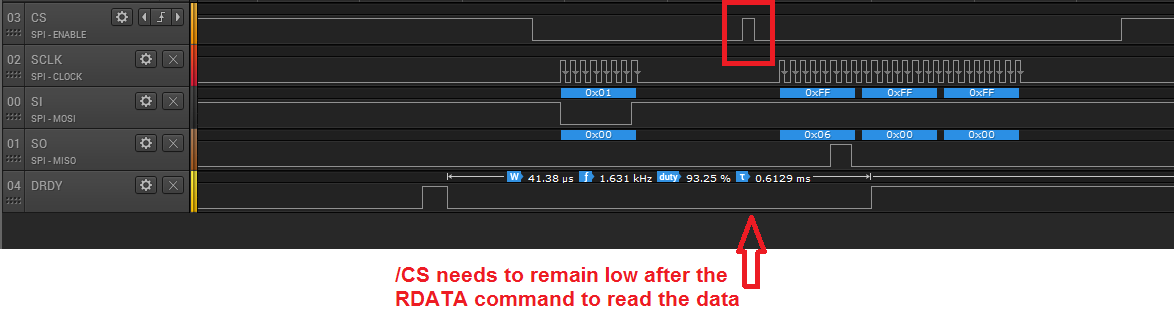
Here is logic oscillogram, that shows properly configuration o SPI and ADC (its saleae logic oscillogram with 10 sec length. Its difficult to make screenshot, that provide detailed information about signals). If there is no possibility to open then I'll send a screenshot.
16 MHz, 160 M Samples [22].rar
PROBLEM.
If you look at the trace, you may notice that after 360 ms there is a spontaneous reset. It occurs in different times, and only when reading data. If you configure the ADC and read the data, this is not a problem. The following waveform data without reading.
16 MHz, 160 M Samples [23].rar
On the last waveform reset does not occure.
As this problem occurs when any attempt to change source at the input. I have suggested that it may be either a defense mechanism within the ADC from the ESD or any another overvoltage, but I did not find anything in the datasheet.
Please any help in solving the mystery. Thank you!
With respect,
Maslov Artem