This thread has been locked.

If you have a related question, please click the "Ask a related question" button in the top right corner. The newly created question will be automatically linked to this question.

ADS8422 input signal concern and VCC applied THS4131 concern

Other Parts Discussed in Thread: THS4131, ADS8422, THS4031, ADS8411

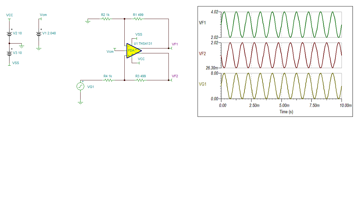
I am using this ADS8422 and my concern is that my input signal will be changing to a max voltage from 0V to 10V to the THS4131 op-amp before the ADC. The datasheet specifies that the maximum you can have applied to +IN and -IN is -0.2 to Vref+0.2V. I have the ADC set to "Single-Ended Driving Circuit for When Input is Single-Ended Unipolar and has Common-Mode of 2.048 V". I was wondering if there is a way to set the Common-Mode to higher than 2.048V using this configuration. 

 I am driving the ADS8422 with the op-amps THS4131. based on the VCC datasheet, the VCC can be set to +15V and -15V. I have them connected to VCC=+12V and -VCC = -12V. I was wondering if I need to limit the rail on the opamp so I do not damaged the ADS8422 since a maximum of 10V signal will come to the input of the op-amp

Please let me me know how I can configure this ADC properly so my input signal is not compromised.

  • Hi Maynor

    You can go up to 8Vpp around Vcm when input signal is signle ended unipolar. Please refer to Figure.30 of ADS8422 datasheet. This circuit is doing single ended to differential conversion and you can have signal swing of 8Vpp around Vcm. You can not go beyond 8Vpp as ADS8422 internal reference is 4.096V.

    You can attenuate signal from 10V to 8V before it reaches to ADC input. This can be done by adjusting gain setting resistors in THS4031 signal conditioning stage.

    Can you please let me know below details about ADC

    1. What is the sampling speed required

    2. What is the maximum frequency of input signal

    Based on your inputs we can look at other possible option from SAR portfolio which is best suitable for your requirement

    Thanks & Regards

    Abhijeet Godbole

  • 1. We need ADC to sample higher than 1MHz, have have parallel communication, SAR. I went through your entire catalog but I assume you have a better way to search for ADCs.

    2. It is aroung 250kHz. (My boss like to over design)

    I am Ok using configuration on Figure 30. I can also clamp the my voltage to +8V  max. My only question is that my input signal is positive so I will attach it to +VIN. That means I connect to -VIN to GND? I should also be ok by using the supply voltage to be +VCC= +12VDC and -VCC= -12VDC correct?


  • Hi Maynor

    In case of ADS8422 you can not tie VIN- to GND. By doing this you will be violating common mode range on input pins. If you intend to use ADS8422 you have to use single ended to differential driver and meet the common mode range at input of ADC. You also need to restrict ADC input voltage to 8Vpp around Vcm.

    For 8Vpp singal you can go as low as +/- 10V on THS4031 VCC/VSS pins. (See common mode input range THS4031 datasheet)

    I would like to suggest couple of devices that can be suitable for this application

    1. ADS8410: 16 bit, 2MSPS unipolar Fully Differential ADC. Please refer to figure.17 in ADS8410 datasheet. You need to attenuate input signal to Vref (4.096 in this case) in order to meet input full scale range. This device has serial output data format

    2. ADS8411: 16 bit, 2MSPS, unipolar single ended ADC with parallel data interface.

    Please let me know if you find these devices suitable for your application

    Thanks & Regards

    Abhijeet Godbole

  • I cannot use serial communication. It has to be parallel communication.

    Maybe I was not being clear enough. I meant tying -VIN to ground on the input of the op-amp for the differential driver circuit using THS4131.  Not the input to the ADC. See datasheet of THS4131 the configuration in Figure 39. "Fully-Differential Amplifier Using a Single Supply". I am intended to use this configuration for the ADS8422.

    I will restrict my signal to be 8Vpp. where -VIN on the op-amp is tied to ground and +VIN is my input signal. Then the +IN and -IN differential output goes to the ADC. Will this work?

  • Hi Maynor

    Thanks for the clarification.

    Full scale input range for ADS8422 input pins is rated for Vref (4.096V). That means differential input voltage at ADC input pins should never exceed Vref (4.096V)

    In your case input voltage at op-amp input is 0 to 8V single ended. You can use figure.39 in THS4131 datasheet but need to make sure you attenuate this o to 8V singal to 0 to 4V so that ADS8422 input specification is met. This can be achieved by having gain of 0.5 in THS4131 stage. Please see attached simulation results with THS4131. You can simulate this circuit with TI-TINA if needed.

    I hope this helps. Please let me know if you have any questions

    Thanks & Regards

    Abhijeet Godbole

  • I will definitely try this configuration.

    Thank you for all your help.  I really appreciate it.