This thread has been locked.

If you have a related question, please click the "Ask a related question" button in the top right corner. The newly created question will be automatically linked to this question.

ADS1120 Maximum Sample Rate with four channels

Other Parts Discussed in Thread: ADS1120

Dear all,

I'm trying to get the fastest possible sample rate when using four channels on the ADS1120. However, the channels seem to influence each other.

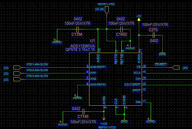
The system is set up for 2000 SPS in turbo and single-shot mode with gain 64, frequency of the SPI is 1.5 MHz. The measurement is done in the following order:

1. ANIN0 - ANIN3
2. ANIN1 - ANIN3
3. ANIN2 - ANIN3
4. internal temperature sensor

The following SPI commands will be sent:

0x40-0x2C-0xD0-0x40-0x08 - wait 870 µs - 0x40-0x4C-0xD0-0x40-0x08 - wait 870 µs - 0x40-0x5C-0xD0-0x40-0x08 - wait 870 µs - 0x40-0x00-0xD2-0x40-0x08 - wait 2.25 ms - repeat

If I'm changing the input value on channel 2, the value on channel 3 is changing slightly, too.

To find out the reason I tried to sample always the same channel 2:

0x40-0x5C-0xD0-0x40-0x08 - wait 870 µs - 0x40-0x5C-0xD0-0x40-0x08 - wait 870 µs - 0x40-0x5C-0xD0-0x40-0x08 - wait 870 µs - 0x40-0x5C-0xD0-0x40-0x08 - wait 2.25 ms - repeat

But even with this I got different results:

Channel 1: -106 digits
Channel 2: -172 digits
Channel 3: -185 digits
Channel 4: -188 digits

If I'm changing the wait time from 870 µs to 5 ms the four results will be equal to -100 digits, which is the correct result according to the input voltage.

Can anybody explain this behaviour?
Is there a settling time required between changing the channel and starting the conversion?

  • Hi Ralf,

    Welcome to the forum! I believe the issue is related to the communication, and you are actually running at a different data rate than you think you are running.  It appears that you are attempting to write 3 registers starting at register 0, and then issue the START/SYNC command.  Instead, the command you are using is write 1 register starting at register 0. The correct register write (WREG) format is shown in Table 14 of the ADS1120 datasheet. In short, the correct command for writing 3 registers starting at register 0 is 0x42 (format 0100 rrnn, where rr is the starting register and for register 0 rr = 00 and writing 3 registers nn = 3-1 so binary nn = 10 which is the number of registers you want to write  minus 1).

    Best regards,

    Bob B

  • Hi Bob,

    Thank you for your answer. Unfortunately there was a typo mistake since I really had used the 0x42 for writing the registers. Meanwhile I found the problem with my setup sampling always the same channel. The SPI sequence was not like expected. Sometimes it was restarted in between the sequence. With the correct sequence I get the same result on all four channels.

    However, the original problem with influencing channels still exist with the following configuration:

    1. ANIN0 - ANIN3, PGA disabled
    2. ANIN1 - ANIN3, PGA disabled
    3. ANIN2 - ANIN3, PGA enabled with gain 64
    4. internal temperature sensor

    Sampling this configuration with the above sequence gives different results on channel 3 depending on the value of channel 2. For example, with 0 V on channel 2 I get -100 digits on channel 3 but with 1.5 V on channel 2 the result on channel 3 is +800 digits.

    So I added a delay between changing the channel configuration and starting the conversion of approx. 4.8 ms. With this delay the result on channel 3 is nearly the same independant of the voltage on channel 2.

    Is there any settling time required when changing to a channel with PGA enabled?

    Do you have any idea how to make this process faster because with the additional delay I need almost 20 ms to sample all four channels (requirement is less than 5 ms for four channels)?

  • Hi Ralf,

    This sounds like analog settling to me.  Do you have a schematic you can share?  Can you tell me more specific information regarding what is connected to the inputs?  The information you are now providing is much different than the information you posted previously. What are you using for a reference?

    If you are using PGA disabled for the first two channels, I will assume that you are attempting to measure close to the supply rails. You must make sure all measurements are within the common-mode input range for the ADS1120. If AIN3 is close or at AGND, then you will have an issue.  Also, with the PGA disabled there is a switched cap input and there may be some residual charge leftover from the previous measurement when switching to PGA enabled.

    Unless you need to operate with PGA disabled, it may be best to operate with PGA enabled for all measurements. It would be good to also know if the issue is only seen between channel 2 and 3.

    Best regards,

    Bob B 

  • Hi Bob,

    Please apologize for the confusion. My problem is the influencing of the channels, but during examination of this I found the problem which I described first.

    The schematic is here:

    On each channel 1 (AIN0) and 2 (AIN1) there is connected a 0..5V signal, on channel 3 (AIN3) a signal in the range-5mV..50mV. The reference is 5V connected to REFP0 and AVDD. AVSS is -1.25V.

    Test were made by applying 1.5V separately to channel 1 and channel 2 while channel 3 has -0.25 mV. The influence can be seen on channel 3 if the 1.5V are applied to channel 2, independant of the voltage on channel 1. I see no Influence between channel 1 and channel 2.

    I have tried your suggestion to enable the PGA for channel 1 and 2 with gain 1, but no difference.

  • Hi Ralf,

    I think what you are seeing is due to PGA overload due to operation outside the common-mode input range for the ADS1120.  One observation with respect to the supply voltages, the combined voltage AVDD to AVSS is 6.25V which is outside the recommended operating voltage even though it is within the Absolute Maximum. You have to be very careful not to exceed the absolute maximum of 7V. Transients or drift may result in a higher than expected voltage causing damage to the device.

    Second observation is related to measuring small voltages near analog ground.  This is not a trivial task, and your ground should be a plane area and also be quiet.  Ground bounce can often be an issue.

    As far as the measurement itself, three equations for common-mode must be satisfied. In the ADS1120 datasheet these equations (eq. 13, 14 and 15) are on page 21.  For your channel 3 measurement you need to be mostly concerned with Vcm minimum when using the PGA enabled.  By quick calculation using the mentioned equations, at a gain of 1 you need to have Vcm >= 0.3125 V and at a gain of 64 you need Vcm >= 0.55 V.  As your measurements are relative to analog ground, Vcm for a 50mV input signal is 0.025V which is your highest common-mode and well below the Vcm requirement.

    Even though in time your measurements may settle to a final value, they will be well outside the linear region of the PGA and therefore invalid.

    Best regards,

    Bob B

  • Hi Bob,


    Thank you for your informations.

    We will look what we can change to fullfill the requirements of equation 13, 14, 15.

    Best regards,

    Ralf