This thread has been locked.

If you have a related question, please click the "Ask a related question" button in the top right corner. The newly created question will be automatically linked to this question.

ADS1299 SRB, BIAS and reference

Other Parts Discussed in Thread: ADS1299

Hello,


I am designing a modular EEG. This means that up to 5 separate (but identical) boards with ADS1299 could be used, sharing the SPI interface to master board (no daisy-chain will be used).

I have a problem understanding SRB and BIAS pins in relation to reference. I read quite a lot of answers, but I can't quite make sense of everything.

I would like to have the same reference for all of the boards, but due to possible noise interference I can't route the same electrode signal to all. So this probably means that I would have to use a separate reference for each board? Is computing the average reference of all electrodes a viable solution for this? Also in this case I would probably have only single-ended inputs (I would tie IN- pins to GND)?

Other option (which I do not prefer) would be to use a separate reference electrode for each module. If I understand correctly, I would set one of the IN+ channels as reference and the signal would come out of the SRB2 pin, which I would then connect to SRB1, which is connected to all IN- inputs?

And what is the purpose of BIAS pins and how do I use them en each of the above cases? As far as I understand the BIAS pins output a small voltage that then sets the common reference of "measured person".

Also I'm having problems choosing the right connectors and cables. I saw everything from flat cables to special shielded cables. Which one (cable and type of connector for PCB) would you recommend, keeping the price in mind?

Best regards, Jure

  • Hello Jure,

    This is a very interesting problem! Let me first explain what the SRB pins do and what the BIAS pin does. The SRB pins are essentially inputs for a reference input that you intend to connect to multiple channels. The SRB2 pin can be connected to individual channels' positive inputs. The SRB1 pin can be connected to all channels' negative inputs.

    The BIAS pin is the equivalent of a right-leg driver for an ECG measurement. It will output a signal that attempts to keep the patient's common-mode voltage within the valid range for the ADC.

    This datasheet was actually just updated with a helpful section that discusses the various functions of these pins. You can find it here starting on page 65.

    In your case, though, since it is intended to be so modular, I recommend you simply connect all INxN inputs to analog ground (assuming you are using bipolar supplies) and find each electrode voltage in a single-ended fashion. Then you can average each sample to calculate a "reference voltage" to then analyze each individual channel.

  • And how should I handle multiple BIAS output(s)? Should I use only one (from one board) no matter how many boards will be used and leave others disconnected, should I somehow connect all BIAS pins together to one electrode, should I use all BIAS pins (each BIAS pin will be connected to separate electrode) or should I leave all disconnected?

    For calculating reference voltage, I will do as you recommended (I will use +-2.5 V bipolar power supply). I will calculate the average from all electrodes and then recalculate the actual voltage for each channel.
  • Jure,

    Take a look at Figure 51 in the datasheet. This shows how the bias connections of multiple devices should be made. Essentially you should have a single device's BIAS amplifier powered on with the BIASINV pins off all the device routed together. This is because each device's BIASINV pin will have the passive average of all of its BIAS_SENS nets. Tying them together applies the passive average of all devices' BIAS_SENS nets to the input of the single active BIAS amplifier.

    Regards,
    Brian Pisani
  • Hello,

    I almost finished the design, I just need verification if it is ok as it is.
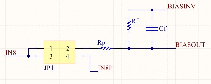
    So I left BIASIN and BIASREF floating. I connect the BIASINV and BIASOUT as in the picture.
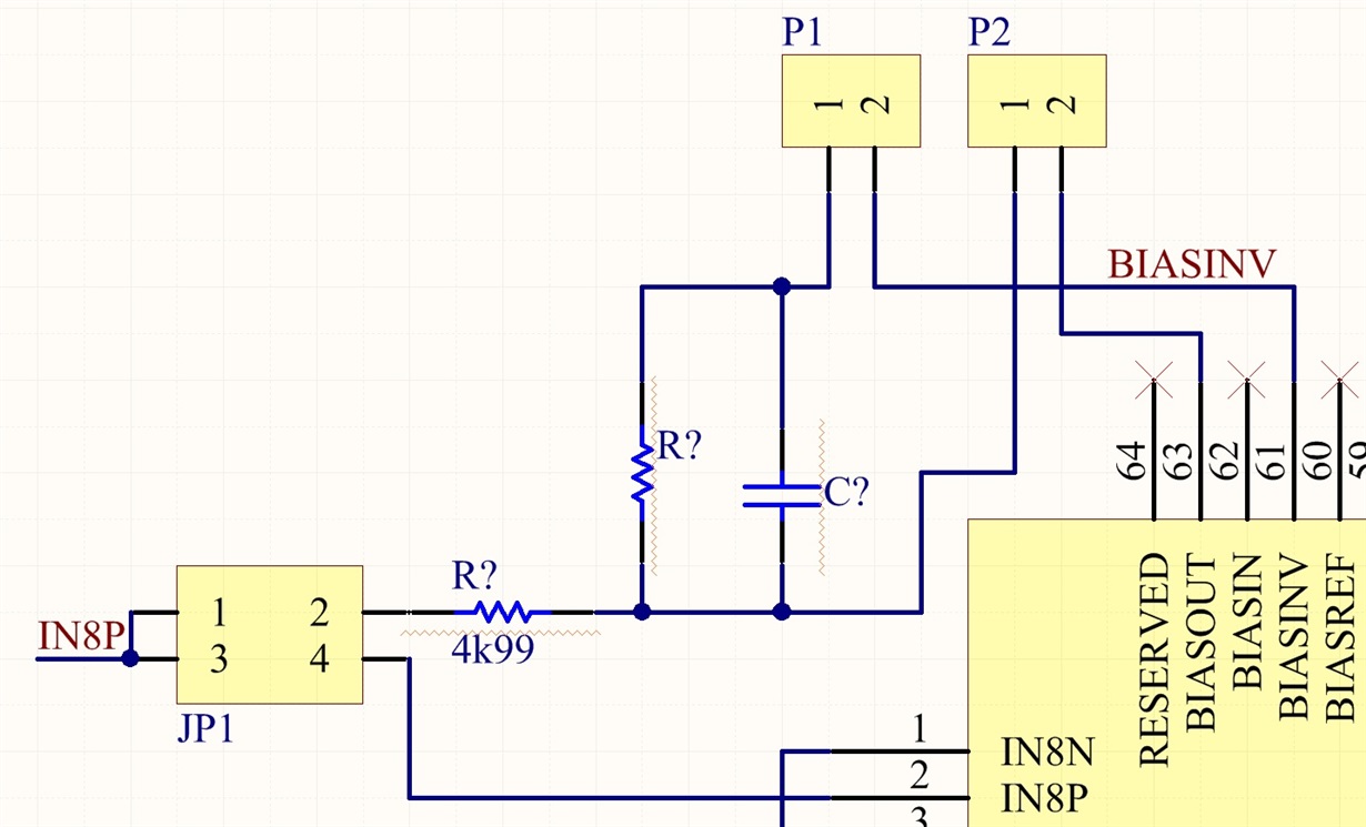
    The jumper is there to select which signal will be at the connector (IN8P input or BIASOUT output). One module will have BIASOUT signal at the connector and all others will have IN8P input. Also all of the modules have BIASINV routed together. The BIASOUT is routed only for each module separately and are not connected together.

    Is it ok if I populate Rf, Cf and Rp on all boards? And then I just power down the bias amplifier on all modules (BIASOUT will be floating i suppose) except the one that will be used for BIASOUT (BIASOUT signal available on IN8 connector)?


    Best regards

  • Jure,

    The only issue that I can see with that setup is that the BISINV pin of a device whose bias amp is disabled will still have an actively driven voltage. I do not believe we have ever tested the impedance of BIASOUT when the amplifier is disabled, so I'm not sure if the BIASINV pin will get loaded by the output of the disabled bias amplifier via Rf. Can you think of a way to easily ensure that BIASOUT of an unused bias amplifier is truly disconnected from the rest of the circuit?

    Brian
  • I can easily add a jumper. In the picture I drew 2 jumpers, only one will be used. I think P1 will be better than P2 since I won't have all of the unused connection (shorter antenna). P1 won't disconnect it from other BIASINV inputs, just the connection from BIASINV to C and R.

    Any recommendation on how to chose R and C values? I found an equation in datasheet, but I am unsure what gain should I set (value of R)? For C I know it sets the bandwidth but I don't know what value should I use.

    Best regards

  • Jure,

    The gain will depend somewhat on your setup since the level of mismatch between the electrode connections will depend on the type used. I would start with 1 MOhm and see what kind of CMRR you can get. If you can't get enough, increase the size of the resistor. The only issue with using too much gain is that if the op-amp saturates there will be some delay in recovery. This delay will make it more difficult for the amp to act as the control mechanism as it is intended.

    The reason you want to limit the bandwidth is because the capacitance in the cable can create a pole in the spectrum at a few kHz. This could potentially drive the amp unstable, so it's best to limit the bandwidth to under 1 kHz. However, you must keep the bandwidth larger than the common-mode signal frequency (i.e. 50/60 Hz, 100/120 Hz, etc.) in order for it to cancel those signals. The formula for the bandwidth of the bias amp will be 1/(2*pi*R*C).

    Regards,
    Brian