This thread has been locked.

If you have a related question, please click the "Ask a related question" button in the top right corner. The newly created question will be automatically linked to this question.

ads1248 data read problem

Other Parts Discussed in Thread: ADS1248, ADS124S08

Hello,

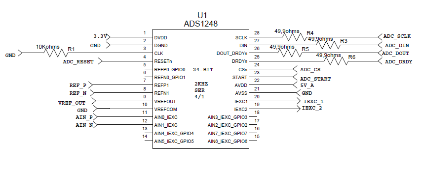
We are using ADS1248 for temprature measurement application. We can cofingure ADS1248 and we have checked that the register settings are correct.

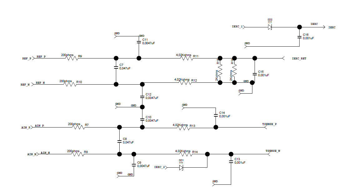
Wu use 500uA current source from IEXC1 and IEXC2, we can see that the current sources work properly.  Our configuration is like 2 wire RTD sense (we connect

IEXC to TSENSE_P and IEXC_RET to TSENSE_N). Since we don't use one of the 2k resistor REF_P and REF_N so for 500uA current for IEXT1 and IEXT2, the expected voltage between REF_P and REF_N is 2 V and we can see it. And  the voltages at AIN_P pin is around 2.8 and at AIN_N 2V.

We have selected REFP1 and ReFN1 as references and AIN0 and AIN1 as input.

But when we read the data by sending RDATA, the converter does not produce any output (gives zero output). What can be our problem?

ADC configuration as follows:

void configureADS1248() {

       //#[ operation configureADS1248()


       // RREG COMMAND 2xh

       // WREG COMMAND 4xh

       // RDATA CMD 14h

       GpioDataRegs.GPADAT.bit.GPIO19  = 0;  // O =LOW, 1 = HIGH


       //SendReceiveSpiA(0x06FF);  // Reset ADS IC

       DELAY_US(100);

       //Stop sending continuous data

       SendReceiveSpiA(0x16FF);


       //DELAY_US(10000);


       SendReceiveSpiA(0x400B);  // WREG CMD and REGISTER ADDRESS  // Number of Bytes to be transmitted -1

       SendReceiveSpiA(0xC000);  // BCS MUX0  // Bias Voltage Register

       SendReceiveSpiA(0x2804);  // MUX1 // SYS0

       SendReceiveSpiA(0x0000);  // OFC0 // OFC1

       SendReceiveSpiA(0x0000);  // OFC2 // FSC0

       SendReceiveSpiA(0x0000);  // FSC1 // FSC2

       SendReceiveSpiA(0x0489);  // IDAC0 // IDAC1


       DELAY_US(1000);

       //SendReceiveSpiA(0x14FF);

       //DELAY_US(4);


}

Rdata :

       ADS1 = SendReceiveSpiA(0x12FF);

       DELAY_US(10); //tcssc = 10 ns

       ADS2 = SendReceiveSpiA(0xFFFF);  // Read Status register 2 (ID)SendReceiveSpiA(0x5A00);  // Read Status register 2 (ID)

  • Dear Murat,

    thanks a lot for considering the ADS1248 for your new RTD measurement design.

    Before I comment on your communication issue I wanted to point a few things out about your design:

    • In case you really only measure 2-wire RTDs there is no need to use both IDACs in your setup. Using both IDACs will actually negatively impact your measurement accuracy. I would suggest to not use IDAC2 in your case. You also save power and one diode in your case this way.
    • We usually show a full common-mode and differential mode filter on the reference input in our example circuits. However you might be just fine with a simple differential capacitor on the reference inputs. Although you might need the series resistors on the reference inputs in case you need to protect those inputs from over-voltages - at least at the REF_P input because the REF_N input would be already protected through the 2kOhm reference resistor.
    • Do you have a capacitor in the range of 1uF to 47uF connected between VREFOUT and VREFCOM?
    • What are the 200R resistors needed for?

    Your communication looks correct to me.
    One thing I suggest in your case is to set the device into SDATAC mode by issuing the respective command right at the beginning.

    I have difficulties to follow your code to be honest, but I believe you don't see any conversion results because the ADS1248 might not be converting.

    • When do you take the START pin high? The START pin needs to be high in order for the ADS1248 to convert.
    • Also do you trigger on the falling edge of /DRDY to know when to read a new conversion result?
    • Do you see /DRDY toggling at all? This will tell you if the device is converting.

    As a last comment I also wanted to make you aware of a new device which we will release this month. It is called the ADS124S08 which is the next generation of the ADS1248.

    Regards,

  • Dear Wurker,

    I am a colleaque of Murat, we work together. As for the issues related with software,

    The start pin is configured as high as soon as the power is on.

    Having configured the registers, and read back correctly the DRY pin toggles as expected, which indicates that a new conversion is completed, as you have emphasized above.

    Since we are sure that the device functions properly(Since we could manage to read back the register values, the desired current outputs are right and data sampling rate is accurate), we look for the falling edge of the DRY pin and having recieved the interrrupt, RDATA  and 3 NOP commands are being sent respectively.

    The problem is, if we are sure that the device is configured correctly, data are converted as DRY pin toggles,what may be the reason for us to get only 0x000000 as an DOUT output drom the device.

    Could you share an example procedure so as to read the data properly. 

    Thanks in advance for your attention.

    Gökhan 

  • Gokhan,


    I don't see anything that is unusual. However I did have a few questions.

    First, can you show both a RREG command to verify that you can correctly read back the data from a register? Then show a RDATA command? I would use the oscilloscope to show the /CS, DIN, DOUT and SCLK. Once you get the plots, post them again similar to what you did in the previous post.

    There aren't many cases where you would read all 0s back. Most of the time, if you have a problem, you would read a full-scale value or negative full-scale value if you are reading the ADC value. Getting all 0s is more likely a communication problem. You might be missing the /CS if you get all 0's back or you might have set up the RDATA command incorrectly.

    Do you write to the OSC or FSC registers? If so, I would stop and just use the default values. If either register is far from expected, you might have read issues. It's unlikely that a bad OSC value would give you all 0s, but a bad FSC value might do cause a similar problem.


    Joseph Wu
  • Thank you Joseph,

    You are right. We had problem with FSC and OSC registers . We were writing 0s to these registers (we thougt that their default value is 0).
    When we skip these registers , we manage to read the output value correctly.

    Our fault was :
    SendReceiveSpiA(0x0000); // OFC0 // OFC1

    SendReceiveSpiA(0x0000); // OFC2 // FSC0

    SendReceiveSpiA(0x0000); // FSC1 // FSC2
  • Murat,


    I'm glad that one of my suggestions helped. Note that any time you change the gain on the device, there will be a new FSC setting. I would generally let the device keep this setting. These gain register settings are factory trimmed to get a good gain error value.


    Joseph Wu