This thread has been locked.

If you have a related question, please click the "Ask a related question" button in the top right corner. The newly created question will be automatically linked to this question.

ADS7841 conversion timing

Other Parts Discussed in Thread: ADS7841

Hello,

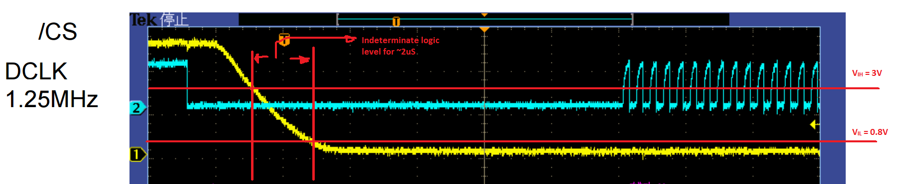
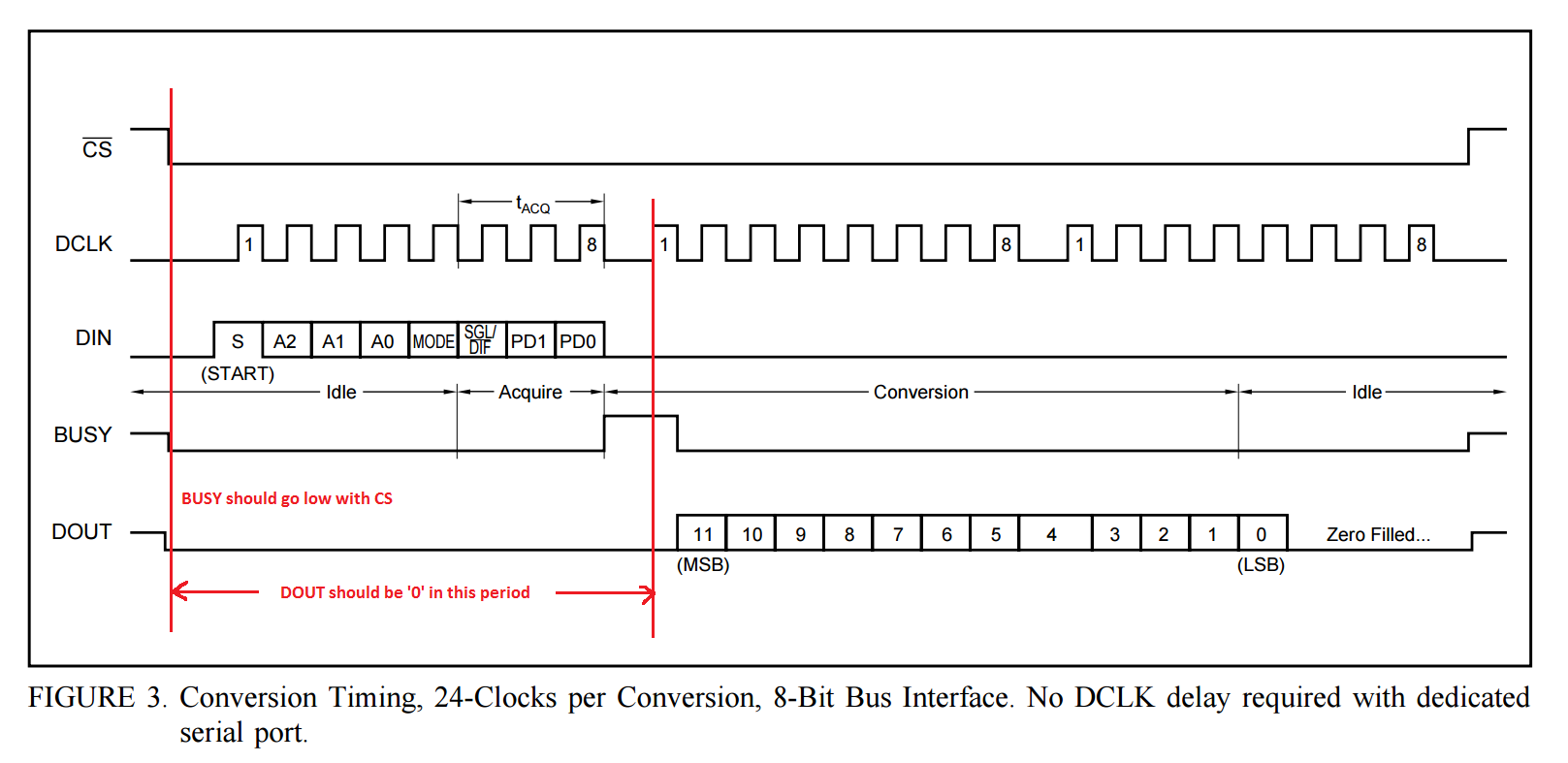
Our customer use the ADS7841.

The BUSY pulse occur at after 8 clocks. 

In sometime, it occur at after 11 clocks.

Is it correct?

The configuration of the customer as follows.

 12bit conversion mode

24clocks per conversion

Best Regards,

Naoki Aoyama

  • Hello Aoyama-san,

    Getting BUSY pulse after 11 clocks is not expected.
    Could you please share oscilloscope shots in the fault and working conditions for these pins - DIN, CS, SCLK and BUSY?

    Regards,
    Rahul
  • Hello,

    Thank you for your reply.

    I attach the oscilloscope shots.

    ADS7841_conversion.pdf

    Regards,

    Naoki Aoyama

  • Hi Aoyama-san,

    1) I think there is a hold time violation on the DIN line with respect to SCLK. DIN should be valid at least 10ns after SCLK rise edge. Please see the image below.

    2) In this case, the device has taken clock number 4 as the start bit. 8 clocks after this edge BUSY goes high. Hence the observation that BUSY goes high after 11 clocks.

    3) You could try the following things

    a) Launch SCLK sooner than what it is right now. Or you could delay DIN by 100ns. This will fix the hold time violation.

    b) You could slow down SCLK. 

    Please check if this helps.

    Regards,
    Rahul

  • Hello Rahul-san,

    Thank you for your fast reply.

    I have an another shot, another channel.

    ADS7841_conversion2.pdf

    The BUSY pulse occur after 11 clocks, too.

    I will ask the customer to input slow CLK.

    Regards,

    Naoki Aoyama

  • Hi Aoyama-san,

    Based on the second capture, I have two more recommendations.

    1) Please capture the frame from CS falling edge to CS rising edge. This will show the full frame.
    2) Please keep DIN low before CS falling edge as per Figure 3 of the datasheet.

    Regards,
    Rahul
  • Hi Rahul-san,

    Thank you for your fast reply.
    I will ask the customer to get a new shot.

    Regards,
    Naoki Aoyama
  • Hi Rahul-san,

    The customer checked the DIN Low start. The issue is clear.
    The BUSY pulse always occur at after 8 clocks.

    What is the difference between DIN Low start and DIN High start?
    Is there any timing specification about the CS and DIN?

    Regards,
    Naoki Aoyama
  • Hi Aoyama-san,

    The control byte starts when it detects the "first" high bit on DIN. This is the description of "S" bit.
    Hence, DIN must be held low during start of frame i.e. CS falling edge. 

    If we refer to Figure 4, it can be seen that DCLK can be high or low at CS falling edge, however DIN has to be low. I understand that this aspect is not very clearly highlighted in the datasheet, unless we specifically refer to Figure 4 and notice DIN.

    Thank you for providing the oscilloscope shots which were immensely helpful in understanding the query.

    Regards,
    Rahul

  • Hi Rahul-san,

    Thank you for your support.
    I will explain the customer this information.

    Thanks,
    Naoki Aoyama
  • Hi Rahul-san,

    Allow me to ask one more question.

    The customer fail to convert sometime.

    It occur at after the supply voltage start up.

    Is there any sequence or initialize at first CS High to Low?


    I will ask the customer the scope shot.


    Best Regards,

    Naoki Aoyama
  • Hi Aoyama-san,

    Could you please share the specific nature of the failure?
    Is the read-out invalid or BUSY pin does not indicate conversion status after 8th clock?

    Regards,
    Rahul
  • Hi Rahul-san,

    Thank you for your reply.

    I attach the oscilloscope shots.

    ADS7841_conversion3.pdf

    When the CS is High to Low, the BUSY pin remain High.

    I'm worry a slow rise and fall edge is OK.

    The customer use a pull-up resistance as 4.7kohm like I2C communication.

    Is it OK?

    Best Regards,

    Naoki Aoyama

  • Hi Aoyama-san,

    As you pointed out, the digital interface is misbehaving because the CS pin is remaining in indeterminate state for too long. If you notice the timing on CS pin, it is indeterminate for over 2us.

    The pull-up resistance on CS pin should not be a problem as long as the driver is able to drive the capacitance on the CS pin trace on the PCB.

    Looking at the CS falling curve, it almost seems like there is a large capacitance or resistance on this pin. Or alternately, the pin is not being driven low, it is being floated. As other digital pins do not have such a slow slew, could you please confirm as to how the CS pin is being driven?

    Regards,
    Rahul

  • Hi Rahul-san,

    Thank you for your fast reply.
    I will check the customer how about drive the /CS pin.

    Is there any spec about the rise/fall time of /CS pin?

    Regards,
    Naoki Aoyama
  • Hi Aoyama-san,

    There is no specific timing requirement on CSn fall/rise time. However, if the CSn pin is in indeterminate state for a considerable time, different pieces of internal logic will interpret the CSn pin logic level differently. Hence they may run out of sync.

    Please correct me if i have missed something - but this problem seems to be related to CSn rise/fall time and not the device power-up.

    Driving CSn just as DIN and DCLK are driven in the attached oscilloscope plots should help.

    Regards,
    Rahul
  • Hi Rahul-san,

    The customer checked with the /CS rise/fall time quickly by using comparator.
    But the results were no change.
    I ask the customer to share oscilloscope shots.
    I will attach the shots later.

    Regards,
    Naoki Aoyama
  • Hi Aoyama-san,

    Thanks for the update.

    Regards,
    Rahul

  • Hi Rahul-san,

    The customer send me the results.

    I attach the file.

    ADS7841_conversion4.pdf

    Regards,

    Naoki Aoyama

  • Hi Aoyama-san,

    Thank you for the oscilloscope plots. The CSz signal has clean transition just as other digital signals.

    In the oscilloscope plots, DIN and SCLK pins are not held low throughout. They are pulled low before CSz goes low.
    Could you please ensure, DIN and SCLK are low when CSz is inactive.

    Regards,
    Rahul
  • Hi Rahul-san,

    Thank you for your reply.
    I will ask the customer to test again.

    Regards,
    Naoki Aoyama
  • Hi Rahul-san,

    It is almost clear by change the DIN signal input trigger.

    I attach the results.

    ADS7841_conversion5.pdf

    When the first High bit on DIN, BUSY is High to Low.

    I want to confirm the sequence after power on.

    1) /CS High to Low

    2) DIN Low to High (first high bit)

    then conversion start. Is this correct?

    I ask the one more question about Page 3 on the attach file.

    The DOUT output some signal in first control byte after power on.

    Is there any power on reset for DOUT?

    Best Regards,

    Naoki Aoyama

  • Hi Aoyama-san,

    Thanks for providing the oscilloscope plots.

    The device timing is expected as shown in figure below,

    1) BUSY should go low along with CS. In the plots which you sent, BUSY is going low with first high bit on DIN. This is not expected.
    2) DOUT should be at logic 0 during the first 9 SCLKs. In the plots which you sent, DOUT is toggling in this period. This can happen if you operate the interface as shown in Figure 6 of the device.

    Could you please capture the oscilloscope plots in the following configuration,

    1) Capture two conversion frames.
    2) Ensure DIN is low when CS is high. Default state of DIN should be logic 0. DIN should toggle as per Figure 3 of the data-sheet.
    3) Ensure DCLK is low when CS is high. Default state of DCLK should be logic 0.
    4) I noticed, there are 25 SCLKs being in the conversion frame. Could you please change that 24?

    Regards,
    Rahul

  • Hi Rahul-san,

    Thank you for your opinion.
    I will ask the customer the plots in that configuration.

    Regards,
    Naoki Aoyama
  • Hi Rahul-san,

    The customer send me the oscilloscope plots.

    I attach the file.

    ADS7841_conversion6.pdf

    It seems OK after 2nd conversion.

    The customer input DIN data High after send control byte. Is it OK?

    Regards,

    Naoki Aoyama

  • Hi Aoyama-san,

    Thanks for the oscilloscope plots.

    1) Now that DIN and SCLK are low when CS is high, the BUSY pin behaviour is normal.
    2) DOUT pin having data on its output during the first 8 SCLKs during the 1st and 2nd conversion is not expected.

    Could you please confirm the following -

    • If the data-out is valid starting from first conversion.
    • During device VCC ramp-up, what is IO level of CS, DIN and SCLK?

    Regards,
    Rahul

  • Hello Rahul-san,

    The customer check the IO level during VCC ramp-up.

    The customer use individual voltage source for ADS7841 and MCU.

    The results is unsolved. In sometime, the BUSY remain high whichever the IO

    level high or low.

    ADS7841_conversion7.pdf

    Do you have any idea?

    Best Regards,

    Naoki Aoyama

  • Hi Aoyama-san,

    From what I see in the oscilloscope plots, you are getting some bits on DOUT during the first 8 SCLKs. However, this zone is to be ignored by the host because no ADC data is expected in this period.
    Valid ADC data starts after busy goes high-low during the 9th SCLK.

    Looking at the ADC data, do you see any discrepancies in the output values?

    Regards,
    Rahul
  • Hi Rahul-san,

    Thank you for your reply.
    The customer's configuration is
    Vref=4.993V , Vin=0.01~0.02V
    so, DOUT output data after 9th SCLK is correct.
    I do not see any discrepancy.

    What is the DOUT output some data before 8th SCLK?
    It is occurred every conversion.
    It seem occurring at least for the acquisition time.
    Is it a just design?
    Of course I will suggest the customer to ignore this effect.

    Regards,
    Naoki Aoyama
  • Hi Aoyama-san,

    I am sorry for the delayed response as I was away for a while.

    The timing diagrams in the datasheet are not very clear about what to expect on SDO when command frame is being sent on SDI prior to a conversion start. Hence it is best you ignore the SDO line during this period i.e. the first 8 clocks.

    Regards,
    Rahul