This thread has been locked.

If you have a related question, please click the "Ask a related question" button in the top right corner. The newly created question will be automatically linked to this question.

Can ADS5400 use DC-coupled to sample signal from -2V to 0.5V?

Other Parts Discussed in Thread: ADS5400, LMH5401, TSW12J54EVM

Now I am using two ADS5400 to sample the signal, which is from -2V to 0.5V, and should use DC-coupled.


How can I achieve it? Can you give me some advice? Thanks.


Also there is another requirement: the difference of the two ADC devices must below 25 ps, Can the ADS5400 achieve it?


Best wishes!

  • Hi,

    The analog input must be fully differential about a common mode voltage of 2.5V, so with a differential peak-to-peak full scale range of 2V that means that the input voltage at each pin of the differential input must be in the range of 2.0V to 3.0V.   (differential peak to peak of 2V means the peak to peak of each side of the differential would be 1V, and with a 1V peak to peak centered about 2.5V that means the signal swings from 0.5V below VCM to 0.5V above VCM.)

    You would need to have some sort of signal conditioning circuit to transform the signal that you have into a signal that conforms to the requirements of the analog input of the ADC.   if you didn't need DC coupling, then a transformer would be a convenient way to convert a single ended signal to balanced symmetrical differential and also provide AC coupling so that the signal could be biased up to VCM after the transformer.   But a transformer would not pass DC, so if you require DC coupling then a differential amplifier circuit of some kind would be required.  Your signal is large enough that a gain factor is not required in the amp, and in fact a little attenuation would be required to get a 2.5V swing down to 2V max, but still a differential amp circuit would be required to output a differential signal at an output common mode of 2.5V.

    For the second requirement, if the difference you want is difference in aperture delay from the clock edge to the sampling instant, then that may be an issue.  The typical aperture delay is 250ps, with a minimum and maximum not specified.   So a device to device variation in aperture delay of under 25ps is not likely.

    There is however the ability to adjust the aperture delay through register writes through the SPI interface.  There is a coarse clock phase adjustment register with 5 bits of adjustment for 32 clock phase settings, and each coarse clock phase step is nominally 2.4ps.   So there is a range of about 73ps of aperture delay that can be adjusted for each device.  Plus another 7 ps of fine phase adjustment.     But it would be up to you to have a way of calibrating your system with some way of measuring the aperture delay mismatch between two devices so as to be able to know what setting to apply to the SPI phase adjustment registers.   For example, if you input a calibration signal to both devices and look at the output of each ADC to see how much they differ and adjust the phase delay accordingly.

    Regards,

    Richard P.

  • Thanks for your replay.
    Why differential peak to peak of 2V means the peak to peak of each side of the differential would be 1V, and with a 1V peak to peak centered about 2.5V that means the signal swings from 0.5V below VCM to 0.5V above VCM?
  • Because if a single ended signal swings from (VCM - 0.5V) to (VCM + 0.5V), then the peak to peak swing on that single ended signal must be 1V.    And a differential peak to peak swing will be twice that of a single ended signal.      Example, for a differential signal when the IN+ signal is at 2.0V and the IN- signal is at 1.0V, then the differential voltage is +1V.    But when the IN+ signal is at 1.0V and the IN- signal is at 2.0V, then the differential voltage is at -1V.    So the differential voltage swings from -1V to +1V for a peak to peak swing of 2V differential. 

    Regards,

    Richard P.

  • Thanks for your help.

    In 7.3.10.1 of ADS5400's datasheet, "A signal gain adjustment is avaiable in registers 0x00 and 0x01. The allowable fullscale range for the ADC is 1.52-2Vpp can be set with 12-bit adjustment resolution across this range".

    So, the AINP and AINN is 1.74Vpp-3.26Vpp or 1.5Vpp-3.5Vpp?

    Thanks.
  • Hi,

    You are still off by a factor of two.  The full scale range of 1.52V to 2.0V is *differential* peak to peak.  

    For a full scale range of 1.52V differential peak to peak, the voltage swing on each side of the differential pair would be 0.76V centered about the VCM voltage.  That means that each side of the differential pair would swing from 0.38V below VCL to 0.38V above VCM.  That would be between 2.12V to 2.88V if VCM is 2.5V. 

    Regards,

    Richard P.

    Richard P.

  • Thanks for your hlep.

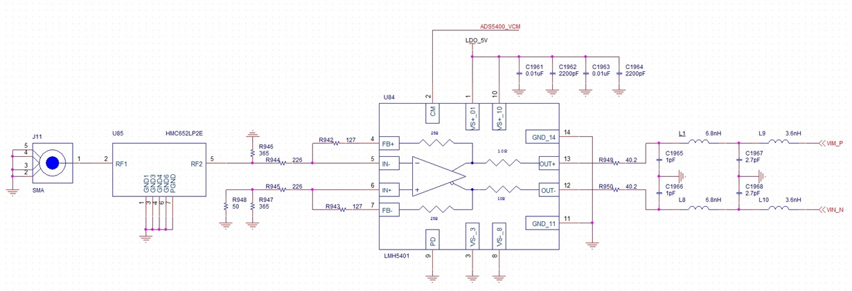
    I think I can use LMH5401 to change the input signal.

    The above configuration is from TSW12J54EVM.

    The CM pin of LMH5401 is link to ADS5400's VCM output voltage, and this is 2.5V.

    The VS+ of LMH5401 is 5V, which is generate from LDO power supply, and VS- of LMH5401 is link to GND.

    The gain of LMH5401 is = Rf/Rg=(25+127)/226=0.67

    If input signal is out of the ADC input, I use a HMC652LP2E to Attenuation the signal.

    Can this work?

    Thanks!

    Best wishes!

  • There is one mistake,

    The gain of LMH5401 is = Rf/Rg=(127+25)/22.6=6.72, I can change the value of the Rf and Rg to make the gain is almost 1.
  • Hi,

    I think this would be the best approach.   I would suggest the high speed amplifier forum would be a better place to review the amplifier circuit itself.   Also, I see that the filter values for the caps in the filter are fairly small (1pF) and as such you may find that your circuit board parasitics are larger than the caps themselves if you're not careful and your filter response may not be quite what you are expecting once you get the boards back. 

    Regards,

    Richard P.