This thread has been locked.

If you have a related question, please click the "Ask a related question" button in the top right corner. The newly created question will be automatically linked to this question.

ADS1220 noise when channel switching at high temperature

Other Parts Discussed in Thread: ADS1220

I'm using ADS1220 in a high temperature Motorsport application to acquire strain gauge and temperature information. The ADC samples from a strain gauge, a RTD temperature sensor, the local board temperature via the internal ADS1220 sensor and ADS1220 amplifier offset and so we are switching between channels using the multiplexer rapidly. At high temperatures (above approx 70 degrees but it gets worse with temperature up to 125 degrees), I start to see significant noise on the strain channel. It appears almost as if the internal PGA cannot settle quick enough and depending which channel was sampled previously affects the strain measurement. See image below:

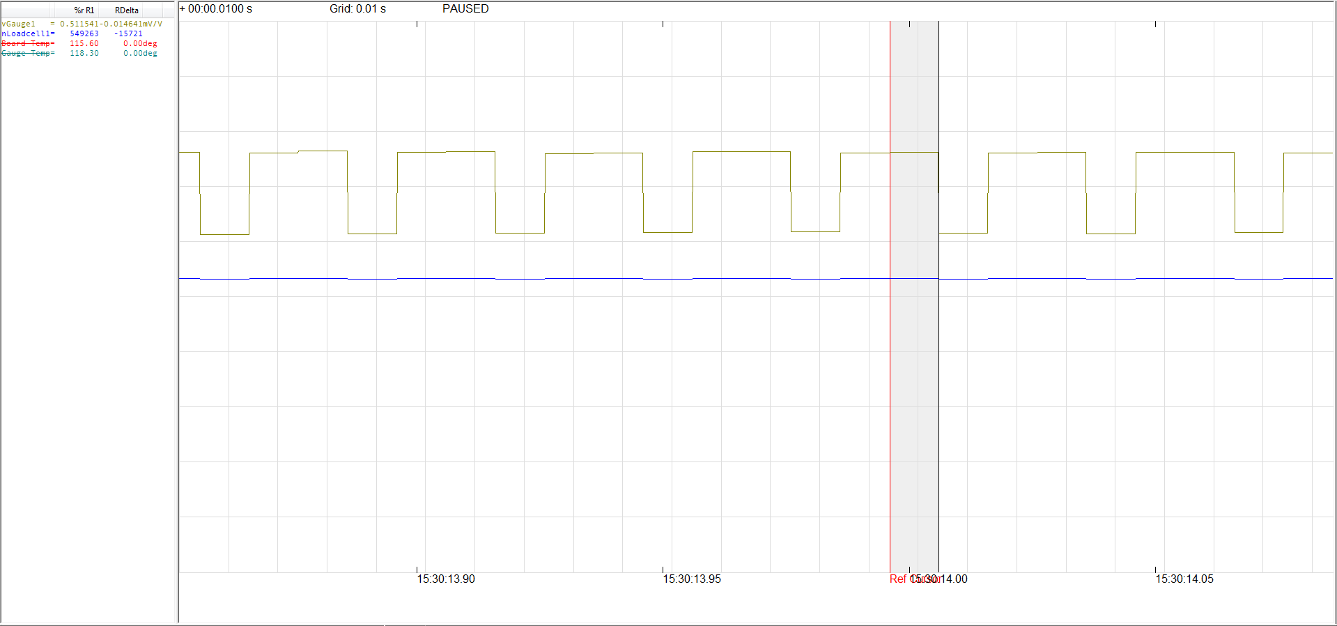
In order to achieve a 200 Hz output data rate with the lowest noise, we are sampling one strain measurement and one "other" measurement per 5 ms cycle. So:

5 ms cycle 1: Sample strain, then sample board temperature.

5 ms cycle 2: Sample strain, then sample ADS1220 offset.. 

5 ms cycle 3: Sample strain, then sample RTD. 

We are using the following register settings for sampling the different channels (register 0, register 1, register 2, register 3):

Strain : {0x3E, 0x70, 0xC0, 0x00}

RTD:  {0xB5, 0xD0, 0xC0, 0x00} 

Board Temp: {0x3E, 0xD2, 0x00, 0x00}

ADS1220 Offset: {0xEE, 0xD0, 0x00, 0x00}

If I disable the other channels (RTD, Temp and Offset) I see very little noise. Similarly, if I add a delay between configuring the ADC for a strain measurement before sending a Start/Sync command, the noise reduces significantly, but to eliminate it I need a 3 ms delay, which makes it hard to sample at 5ms overall. I also note that I see an offset change (14000 counts) if I turn off the other channels. See below:

Are there any settling requirements for the ADS1220 at higher temperatures? Does changing sample rate, PGA gain or PGA enable or reference effect this? From the datasheet, I was under the impression that we could swap between channels with no wait time? I am pretty sure this is going to be something I'm doing wrong, but I don't see it!

Thanks and best regards,

David

  • Hi David,

    Welcome to the forum!  It might be interesting to experiment specifically with your RTD measurement.  As to the other three measurements, there is a great degree of similarity and I wouldn't expect to much shift here accept for temperature drift.

    The RTD measurement is a bit different in a number of ways as it uses PGA bypassed at a different gain.  This measurement channel also uses AIN3, which has a MUX connection to AVSS.

    What happens to the device over temperature is shown in the graphs of the ADS1220 datasheet starting on page 10.  One thing to note is the offset voltage will increase within the temperature ranges you mentioned.  Another thing to note are the graphs on page 12 showing absolute input current versus input voltage.  In Figure 18 for 125 deg C, you can see that AIN3 input current has increased significantly.  The AIN3 increased current is due mostly to the large transistors required for the low-side switch that become much more leaky with increased temperature.

    As to the reason why your measurements are different over temperature is difficult to say for sure as to what the cause is for the error.  It is interesting that adding a delay is making a difference.  This would lead one to believe that there is some settling taking place.  It is possible that there is some settling factor moving from PGA disabled to PGA enabled (or vice versa) moving from a lower impedance to a higher impedance.  It may also be possible, depending on input filtering and device values used, that the additional leakage current may require a settling period for the analog input to settle with the increase in current following the MUX change.  It is for these reasons that I believe the experimentation of taking the AIN3 (RTD) measurement out of the measurement cycle may indicate where the issue is more prominent.

    Is it possible for you to show the schematic?

    Best regards,

    Bob B

  • Hi Bob,

    Thank you very much for your welcome and for your detailed and timely response.

    The change from turning the PGA on and off and changing the gain to read the RTD was an initial suspicion of mine. I also considered whether it was perhaps the measurement of the internal temperature sensor, which uses the internal rather than the external reference. I tried modified code versions to try isolate this where I only performed one of the secondary measurements (only RTD, board temp or offset) together with sampling the bridge to see if one or more of the specific configuration changes were causing the issue. Some were worse than others, but I saw the effect with similar magnitude in all cases.

    Your suggestion of considering the input leakage more closely may be spot on however. The circuit has the standard passive ADC differential input filter with 2 x 4.7k resistors in series with the 1kohm bridge outputs, a 100nF X7R 0402 differential capacitor across the ADC inputs and 2 x 10nF X7R 0201 common mode caps to ground. The caps are a little racy as we are very space constrained on the design (6.5 x 14 mm PCBA including ADC, MCU, CAN transceiver and connections to fit inside a suspension component) and a design decision to choose higher series resistance (4.7k) to allow for smaller capacitor package sizes may be contributing to this issue.

    With the values above and ~10nA differential input current from figure 19 in the ADS1220 datasheet, I get approx ~100uV error due to bias currents (which is in the ballpark). If there is any transient bias current during multiplexer changes, this may pretty much explain the glitching issue.

    I will do some experimentation early next week with different filter components (perhaps a 1uF differential capacitor in a larger package size with 220 ohm resistors). If this is the issue, do you have any other suggestions for perhaps reducing this effect?

    The schematic was also sent to pa_deltasigma_apps@ti.com if anything was unclear above.

    I let you know how this testing goes.

    Thanks again and best regards,

    David
  • Hi Bob,

    Thanks for your help. Testing today with modified filer components showed a significant improvement. We have changed the PCB design to cater for larger package size filter capacitors as well and are also moving from AN1/AN2 to AN0/AN1, which has lower bias current and also better matched bias current.

    I am pretty confident this will sort the issue out completely.

    Thanks again and best regards,

    David
  • Hi David,

    Thanks for the update. If you need any further assistance please feel free to ask.

    Best regards,
    Bob B