This thread has been locked.

If you have a related question, please click the "Ask a related question" button in the top right corner. The newly created question will be automatically linked to this question.

ADS54J60 Fs/4 spur

Other Parts Discussed in Thread: LMH6401, ADS54J60, TSW54J60EVM

Hi,

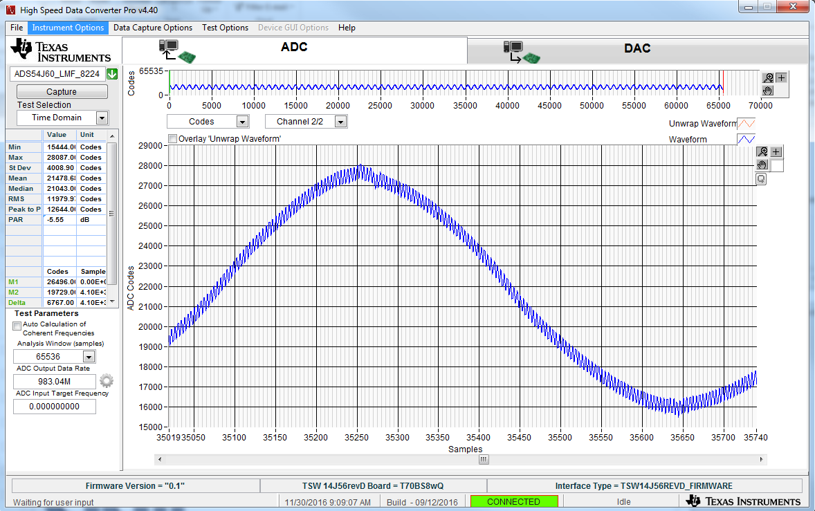
I'm using a TSW54J60EVM and a TSW14J56EVM to evaluate the ADS54J60 and the LMH6401 in DC-coupled mode.  I had to modify the analog front-end from AC-coupled to DC-coupled.  I've removed T1, change C197, C198, C18 and C24  to 0R0 (from 0.01uF series capacitors) and also change R119 to 10K (from 0R0).  

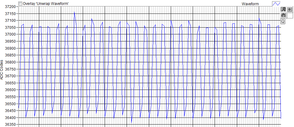
If I inject a DC signal with an amplitude of 0.60V (and over) on J3 and leave J4 unconnected, I get a strong Fs/4 spur (see attach image).  It disappears if the DC signal is lower than 0.60V.

I'm using the default scripts (i.e ADS54J60_LMF_8224.cfg and LMK_Config_Onboard_983p04_MSPS.cfg).

I've tried to modify the EN_INPUT_DC_COUPLING register (Master 80h, x4F) and Nyquist registers (Main Digital 6800h, x42, x4E).  I've also tried to connect the ADC's VCM pin to the LMH6401's Vocm pin (i.e. move 0R0 from R125 to R126).  It didn't fix this issue. 

How can remove this Fs/4 spur ?

Thanks,

Patrice Plante

  • Hi Patrice
    Most of the support team is out of office for the US Thanksgiving holiday. Someone will be able to respond to this early next week.
    Best regards,
    Jim B
  • Patrice,

    Go the TI Design titled "16-Bit 1-GSPS Digitizer Reference Design with AC and DC Coupled Variable Gain Amplifier" using the following link below for more helpful tips with the issue you are having.

    Regards,

    Jim

  • Hi Jim,

    Thanks for the link to the app note!  I've connected the ADC's Vcmo pin to the LMH6401's Vcm pin via a 0R0 on R126.  I've removed R125.  However, I still have the Fs/4 spur when a DC-coupled signal (~1MHz sinewave + 1.7VDC) is applied at J4.  J3 is terminated to 50ohm.  

    At the output of the LMH6401, I've measured at DC offset of 177mV (with Vcm) on OUTP and -185mV (with Vcm) on OUTN.  It looks like the LMH6401 Vcm is shifting as the DC offset increases.

    Can you confirm the component changes to modify the TSW54J60EVM to DC-coupled?  It is not specified in the app note.   Also, the app note shows the two inputs with the same DC-offset when in DC-coupling (see figure 2 in the app note).  Well, I'm confirming that if both inputs have the same DC-offset the Fs/4 spur disappears.  It seems the LMH6401 (in DC-coupled mode) will not keep a constant Vcm when a DC-offset is present at the inputs.

    Regards,

    Patrice Plante

  • Patrice,

    The input should go to J3 not J4 as you mention. Use a 6-dB attenuator on J4 and tie the other end of the attenuator to GND. If you installed R126, you need to remove R21.

    Regards,

    Jim 

  • Patrice,

    I had one mistake in the last post. Use the 6dB attenuator on the analog input (J3), not the return input (J4). The J4 input is already tied to GND by default.

    Regards,

    Jim

  • Jim,

    I've installed R126 and removed R21. I've connected J4 to my input signal via a -5dB attenuator and connected J3 to ground via a 0R0 resistor. The Fs/4 spur is still present, same amplitude and frequency.

    I've also tried to install both R126 and R21. Same results.

    I've tried to connect J3 to ground via a 50ohm resistor. Same results.

    Is there a missing register configuration in the ADS54J60 or LMH6401? Can you reproduce this issue on your side?

    Regards,

    Patrice
  • Patrice,

    Since this is an interleave by 4 device, the Fs/4 spur will always be present. I am checking with the designers to see how low this would normally be. How low is it on your setup and how low do you need it to be?

    Regards,

    Jim

  • Jim,

    The Fs/4 spur jumps abuptly to -36dBFS when there is a DC offset. It is -90dBFs when there is no DC offset. Based on my measurements on the evaluation board, it seems that the LMH6401 output doesn't keep its Vcm to 2.1V. Vcm gets worse (i.e. output is more asymmetric) as the signal propagates thru the low-pass filter.

    IN_BM = 1.370VDC
    IN_BP = 0VDC

    OUTP - VCM = 187mVDC
    OUTN - VCM = -192mVDC

    BINP - VCM = 126mVDC
    BINM - VCM = -142mVDC

    We need the Fs/4 spur at -90dBFS when there is a DC-offset.

    Thanks,

    Patrice
  • Patrice,

    I am modifying a board to duplicate your setup and will repeat your tests. I also forward this post to the amplifier team to see if they have any suggestions.

    Regards,

    Jim  

  • Hi Patrice,

    Based on the voltages you have recorded about the LMH6401 outputs, I think the output Vcm is close to 2.1V. This is because the output Vcm calculation should be VCMO = [(OUTP - VCM) + (OUTN - VCM)]/2 = -2.5mVDC. This means the output Vcm is offset by only -2.5mVDC from the set voltage of 2.1V. 

    I think the ADC should be able to reject the DC offset between the inputs without increasing the Fs/4 spur, unless there is some DC-calibration that occurs at start-up that messes up the Fs/4 spur with the DC offset. I think we will check and get back on this.

    Best Regards,

    Rohit

  • Patrice,

    The offset correction block only has a range of +/-15mV. If DC input exceeds this limit, the device will no longer be able to correct for internal mismatch in DC offset of interleaving cores and Fs/4 spurs will appear in the spectrum. Only way to handle this is to freeze the DC offset corrector with idle channel at ADC’s input. Then apply DC signal. To do this, follow the instructions attached.

    Regards,

    Jim

    ADS54J60_DC_coupling.pptx

  • Jim,

    The fix is working on the TSW54J60EVM evaluation board ! There is still a spur on Fs/4 but it is much smaller as expected. We are going to try this fix on our own prototype board.

    Thanks!

    Patrice
  • Jim,

    The fix also works on our DC-coupled prototype board. Many thanks to you and your team!

    Regards,

    Patrice