A related question is a question created from another question. When the related question is created, it will be automatically linked to the original question.
If you have a related question, please click the "Ask a related question" button in the top right corner. The newly created question will be automatically linked to this question.
As a quick answer, I can think of two things to try.
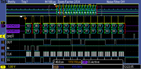
First, before reading the registers, send an SDATAC (03) command. This will prevent the DOUT from being updated with data at every DRDY pulse. It could be that the register read is being corrupted by data being sent to DOUT.
Second, during the read of the register, I would do this with a single CSn low. So, bring CSn low, and issue 10 0B FF ... FF and then bring CSn high again.
One other thing to check (brought up by my colleague Tom Hendrick) is the phase of the read and write.
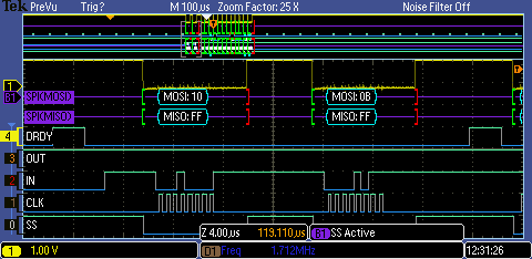
The data is read out and clocked in on the falling edge of SCLK. From your second picture, it looks like you have data clocking in on the rising edge of SCLK.
I do select falling edge of SCLK when I set up SPI bus clock(FYI - I'm using Freescale MCU, MCF51JM connect to ADS1256EVM Board)).
Now it seems better after following your suggestions - bring CSn low, issue SDATAC (0x0F) command and then issue 10 0B FF ... FF and then bring CSn high again. The read out data from registers seems more reliable, but not sure there are correct values... Here is what I've got form DOUT: 0x18, 0x00, 0x00, 0x00, 0x00, 0x00, 0x00, 0x00, 0x00, 0x00, 0x00, 0x00,
For read data from the MUX AIN0, AIN1, it seems the value is not reliable. Here is my pseudo code:
Bring CSn low, issue SYNC command(0xFC); delay 6 us; issue WAKEUP command(0xFF); wait about 6 us; wait until DRDY low; issue RDATA command(0x01); delay 6 us; read data from DOUT (24bit); then bring CSn high again. I did not send WREG command, since I'm only interesting AIN0 and AIN1 input, could that be issue?
I would check your communications again. From your second scope photo, it looks like your DIN is being setup on the falling edge of SCLK for the ADS1256 to be latched in on the rising edge of SCLK.
Second, the reset or default values for the register are given in Table 23 of the ADS1256 datasheet (third column). I'm not sure of all values but depending on the device, they are: