This thread has been locked.

If you have a related question, please click the "Ask a related question" button in the top right corner. The newly created question will be automatically linked to this question.

DAC7750 4-20mA source - Can't get IOUT output with minimum wiring and configuration

Other Parts Discussed in Thread: DAC7750, XTR111, DAC7760

Hi,

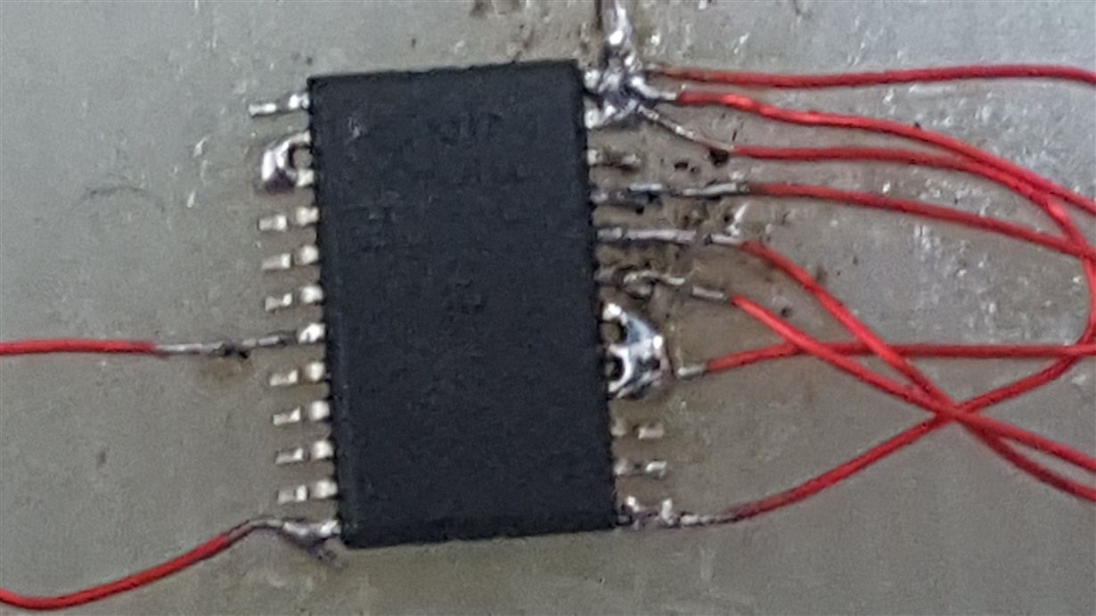
I am having a problem with the DAC7750.  It is not putting anything out on IOUT.  I access the control register and enable the output, the configuration register, and the gain register to give it a gain of 1.  Am I doing anything wrong?

Th bottom right is pin 1.  I have everything connected correctly according to the datasheet.  Also spi is configured with MSB first and sample on rising edge.  The baud rate is low and the hold time is well within specs.

Here is my code:

int main(void)
{
SystemCoreClockUpdate();
spi1_Init();
PORT->Group[0].OUTCLR.reg = PORT_PA19;
spi1_Send(0x55);
spi1_Send(0x10);
spi1_Send(0x05);
PORT->Group[0].OUTSET.reg = PORT_PA19;
for (int i = 0; i < 60; i++) __NOP();
PORT->Group[0].OUTCLR.reg = PORT_PA19;
spi1_Send(0x57);
spi1_Send(0x00);
spi1_Send(0x20);
PORT->Group[0].OUTSET.reg = PORT_PA19;
for (int i = 0; i < 60; i++) __NOP();
PORT->Group[0].OUTCLR.reg = PORT_PA19;
spi1_Send(0x58);
spi1_Send(0x80);
spi1_Send(0x00);
PORT->Group[0].OUTSET.reg = PORT_PA19;
for (int i = 0; i < 60; i++) __NOP();

while(1)
{

PORT->Group[0].OUTCLR.reg = PORT_PA19;
spi1_Send(0x01);
spi1_Send(0xFF);
spi1_Send(0xFF);

PORT->Group[0].OUTSET.reg = PORT_PA19;
for (int i = 0; i < 60; i++) __NOP();
}
}

  • Also, I am powering the chip with 23VDC direct from a power supply. This is the same supply powering my main circuit. There are no decoupling caps and I have not set up CLR or ALARM to work. REFOUT and REFIN are tied together and all grounds are tied together (analog and digital).
  • Emmanuel,

    It is pretty unorthodox to see an IC designed for precision performance in a sort of "sky-bridge" configuration like this. I just want to bring this up because, depending on what your goals are here, this may be an inadequate environment for various performance parameters.

    Have you probed any of these signals to verify that what you believe is happening at the pins is indeed there? Specifically I would suggest that you verify that your intended supplies are indeed present on the AVDD and DVDD pins, since you're using the internal DVDD LDO you should expect 4.6V nominally output on the DVDD pin. For your AVDD supply of 23V I would just suggest that you look at the indicators on the power supply you're using to verify that the rail is indeed there and it is not sourcing an unreasonable amount of current so as to suggest that there was a short somehow created in the setup you have with the magnet wire. Secondary to this I would suggest that you check that the reference voltage output is functional at REFOUT and verify that the voltage is also supplied to REFIN.

    Let's start with these tests to try to verify the setup and move forward based on those results.

    I would also point out that there is an evaluation module for this device that may be helpful for early evaluation or prototyping:

  • First of all, thanks for the quick response. I have verified that the AVDD supply is indeed at 23V. Also the internal DVDD supply is at 4.6V on pin 2. The reference voltage is at 5V for both REFOUT and REFIN. That was before I tied them together as is shown in the picture. I bridged with a bit of solder. Does my code look ok?
    What's a sky-bridge?
  • Also, I used this IC because it has a serial input and a 4-20mA output. I needed a 4-20mA source chip and all I could find was 4-20mA conditioners or sources with way too many bits. Is there another IC you would recommend?
  • Emmanuel,

    A skybridge circuit could very well be some local jargon at the University I attended, but it's basically a term we used to refer to circuits which were basically a bunch of through-hole components soldered to one another without so much as a piece of copper to resemble a circuit-board.

    If you are looking for a fully-integrated device that includes both a DAC and a voltage-to-current converter to derive the current outputs, the DAC7760 and other devices in it's family are the only options (there are 12-bit and 16-bit variants in the family). If you do not need 12-bits of resolution you could use one of the conditioners you mentioned (like the XTR111 for example) along with a discrete 8-bit DAC (or whatever your resolution requirement is) to realize the same current output ranges with a couple of external discrete components.

    As far as the data content in your code goes, it looks fine. But I cannot speak to whether the code successfully outputs the digital signals of interest on your MCU nor that it successfully (and accurately!) delivers these signals to the device. I would suggest you probe the digital signals with an oscilloscope and perhaps share those results on the forum. If you share the captures on the forum please capture LATCH, DIN, SDO, and SCLK all in a single 4-channel oscilloscope capture.

    Another question / test suggestion would be to probe the IOUT pin after the configuration block of your code where you are trying to set the IOUT range to 4-20mA. I would be curious to know if there is 4mA of output current after this block has run. If not, knowing what current is there would also be interesting.
  • Thanks so much for your help.  It appears I had it right all along.  Maybe the IC itself was just faulty.  When I finally received the others, another IC plus some careful soldering appeared to be just what the doctor ordered.  Thanks again for everything.

    Just as an extra question, I was wondering why it doesn't seem to change very quickly when I put the changing value in a for loop?  In fact, when there doesn't seem to be a constant spi data signal, it seems to go back to 4mA.  Is this normal?  Do I have to keep sending the serial command to get anything more than the minimum?  Does it really default back to min right away?

  • Emmanuel,

    Could you quantify how quickly the output value changes and provide details for what the step size is? This would help me understand if the settling time you are observing is expected or not. The specified settling time in the datasheet for a 16mA step size is 10us with no inductive load on the output.

    The device should not require constant SPI writes. My best suspect would be that perhaps the CLR pin is asserted and causing the value to be reset after each write.

  • It does not appear to be asserted but i will tie it low just in case. Thanks for your help.