This thread has been locked.

If you have a related question, please click the "Ask a related question" button in the top right corner. The newly created question will be automatically linked to this question.

ADS1258: The DRDY pin doesn't pluse low

Part Number: ADS1258
Other Parts Discussed in Thread: ADS1278

Hi,

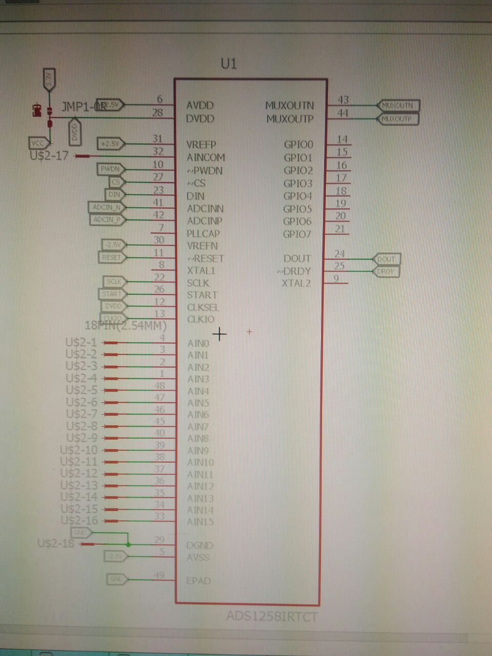
I am evaluating ADS1258, after going through the datasheet I am trying to operate in default mode.

Hardware connections:

DVDD -> 5V

AVDD -> +2.5V

AVSS -> -2.5V

CLKSEL is connected to DVDD.

START, RESET, PWDN kept at logic HIGH state. 

Problem Description:

From what I understand by reading the datasheet is just by giving CLK and SCLK the conversion process should start. I am not writing to any registers as I want to operate in default mode. I gave CLK frequency as 16MHZ and SCLK as 8MHZ. I was expecting the DRDY pin to pulse, but the drdy is always at logic High state.  Where I am I wrong at?

Thank You.


  • Hi Tejas sj,

    Sorry to hear that you are having trouble with the ADS1258. Can you send along a screen shot of the schematic showing the connections to the ADS1258?
  • Hi Tom,

    The schematic is very simple, I have designed a breakout board for ADS1258 for evaluation. The pin connections are as follows:

    CLKSEL pin is shorted to DVDD pin.

    DGNG and Exposed Pad are shorted and used as Ground.

    The pins CS,SCLk,DIN,DOUT,DRDy,START,RESET,PWDN,CLKIO are connected to FPGA.

    Thank You,

    Tejas SJ

  • Hi Tejas,

    Are your analog and digital grounds referenced to the same potential? If not, then the device may not function properly. Otherwise all your other connections and configurations look okay.

    Also after power up, make sure that the clock is running and that the START, /PWDN, and /RESET pins are all set high so that the ADC begins converting. Have you checked on these signals?

    Best Regards,
    Chris

  • Hi Christopher,

    Which pin do I use as analog ground ?

    I have shorted pin no.29(DGNG) and the Exposed Pad and used them as Ground. I have not used any pin as Analog ground.

    The powersupply used are:
    DVDD -> 5V
    AVDD -> +2.5V
    AVSS -> -2.5V

    I had this doubt earlier as I have worked with ADS1278, it has both AGND and DGND. But in ADS1258 there is no different pin as AGND.


    Thank You,
    Tejas SJ
  • Hi Tejas,

    In this case since you're using a bipolar supply, you don't have a dedicated analog ground pin on the ADS1258. However, you'll need to make sure that your analog supplies (that provide AVDD and AVSS) are referenced to the same ground potential as the digital ground.

    Typically, we recommend to dedicating a PCB layer as the ground plane and sharing this ground for both analog and digital grounds. From there you can "partition" the ground plane into analog and digital sections without have to split the ground into separate planes. Designing a PCB in this way can be just as effective at isolating analog and digital return currents (i.e. noise) as using separate ground planes, and also avoids many of the issues associated with split ground planes.

    Best Regards,
    Chris

  • Hi Chris,

    Thank you for your suggestion on a dedicated ground plane for the PCB. I apologize for taking long to reply.
    I have resumed my work on ADS1258. I am still not successful in getting any data out.

    Some of my observations:
    1. DRDY pin is in HIGH logic state at power up. Even when CLKIO,SCLK,PWDN,RESET,START pins are either floating or connected to ground.
    2. I have also toggled the PWDN, RESET, START pin to ground to see no change in DRDY state.

    I have seen this in both the boards I have made. Can you please suggest me the basic test to ensure that the ICs are working.

    Thank You.
    Tejas
  • Hi Tejas,

    The first sign of life to look for is /DRDY going low. If you've properly powered the device, applied the clock, and set the GPIO pins appropriately, then /DRDY should become active. You'll first notice it go low, and then it will begin to pulse at intervals of the ADC data rate (as shown in figure 56 of the datasheet).

    Since you're not using an external crystal on the XTAL1/XTAL2 pins, then you'll need to set CLKSEL high and apply a 16 MHz clock to the CLKIO pin (as shown in figure 40).

    At the moment it would sound like either the external clock or the GPIO pins (START, nPWDN, nRESET) are not configured correctly. I think once you get those set, you'll see the device come to life.

    Best Regards,
    Chris