This thread has been locked.

If you have a related question, please click the "Ask a related question" button in the top right corner. The newly created question will be automatically linked to this question.

ADS7952: Problem with noise on channel 8

Part Number: ADS7952
Other Parts Discussed in Thread: REF3325, , OPA320, OPA625, OPA314, OPA192

Hello

Intro:

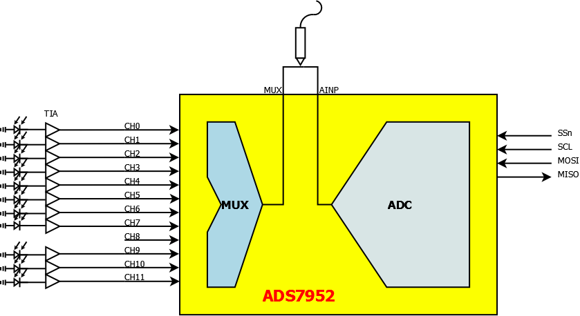
i am designing a board that will have 11 photo-diodes (PD). The PD are connected to transimpedance amplifier (TIA) and the output of TIA is routed to ADS7952 (ADC). The ADC   is configured to run in manual mode with 1MHz as spi clock. The read is preformed every 16.66ms and all channels are read from 0-11. I have chosen REF3325 as my 2.5V ref voltage. I have routed the ADC in buffered mode ... with MUX directly connected to AINP.    

Problem:

When i read all the channels i can see that CH8 is extremely noisy and it has an offset. Even if i apply a constant voltage to all channels i can notice that CH8 shows much lower value. I can not explain my self why. In datasheet i didn't find anything that can explain this behavior of CH8.

Additional Info:

As TIA i am using OPA314. I tried changing for OPA320 and OPA625. OPA625 showed the best performance but there was still a fair amount of noise and offset on CH8. I tried using LTC6268. At this point noise and offset were gone. But LTC6268 has 16mA power consumption and with 11PD that is close to 200mA. That is outside of my power budget? 

Question:


Is there anything special about CH8 that it shows this type of behavior?

If i would to use ADC with buffer between MUX and AINP would the problem go away?

With buffered implementation do i still need 150p cap on each channel?

My board has 3.3V power supply. That means i can not use OPA192 as V-buffer. Can you maybe suggest V-buffer that works at 3.3V and can be used with ADS7952?

Scope Pictures:

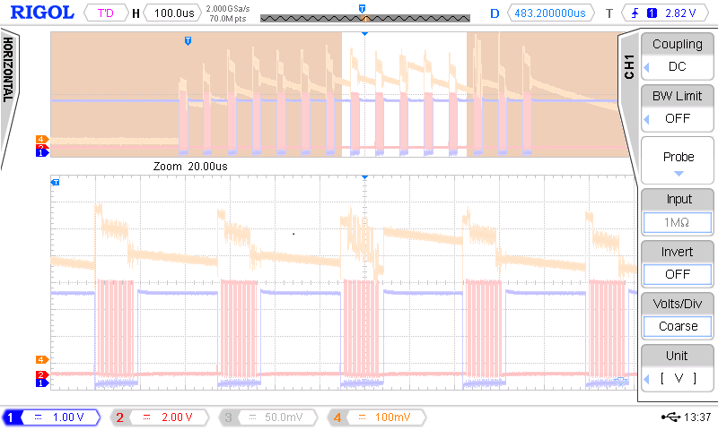
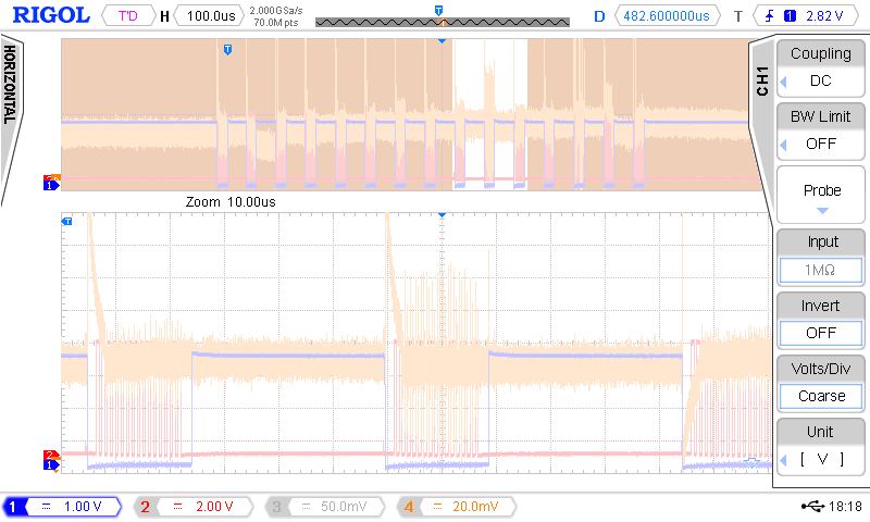
I did some measurements of the board with my scope. I synchronized my acquisition with SSn (purple line). Red line presents the SCK and yellow line is the signal between MUX and AINP.   

As you can see on the yellow line there is much higher noise on 10th SSn low. Interesting is to see that there is no voltage drop which one would expect when ADC shows a offset in the readout.

Next picture present the zoom on the noisy channel

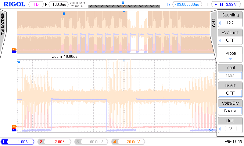
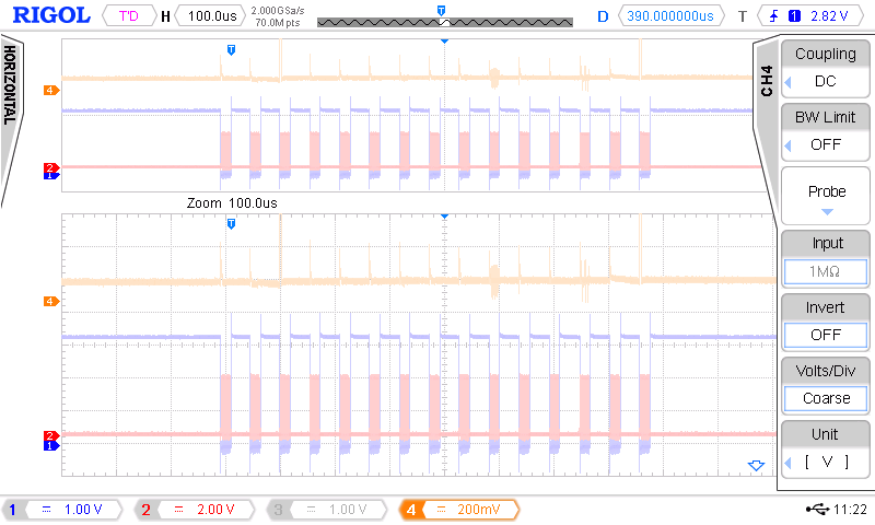
As you can see the yellow line (signal between MUX and AINP) spikes on each transition of the SCK ( red line ). When i compare this to acquisition just before i see no spiking or flickering of the measured signal ( yellow line ). Please see the next picture.

This is zoomed acquisition just one channel before. As you can see there is no noise.

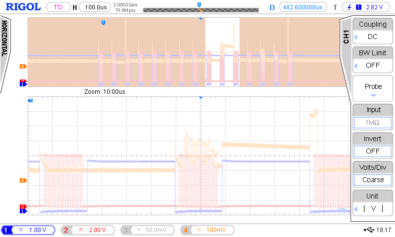
I also acquired SPI signals with my scope. Figure Below:

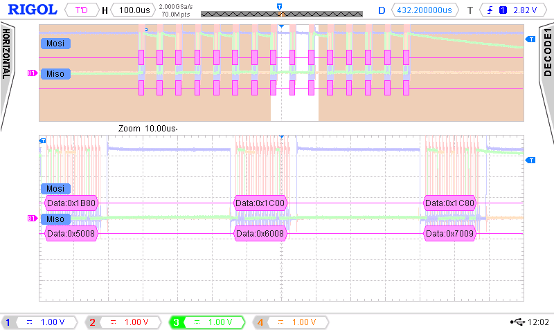
I have zoomed on the 3 acquisitions. I want to show how we are addressing the ADS7952. As you can see from MOSI the channel count is progressing from one measurement to an other. Also MISO shows that ADS7952 is giving us results in progression (first 4 bits of MISO increment correctly). On the last measurement is where i would see the troubled MUX-to-AINP signal.

Thank you very much for your help

Schematic Pictures: 

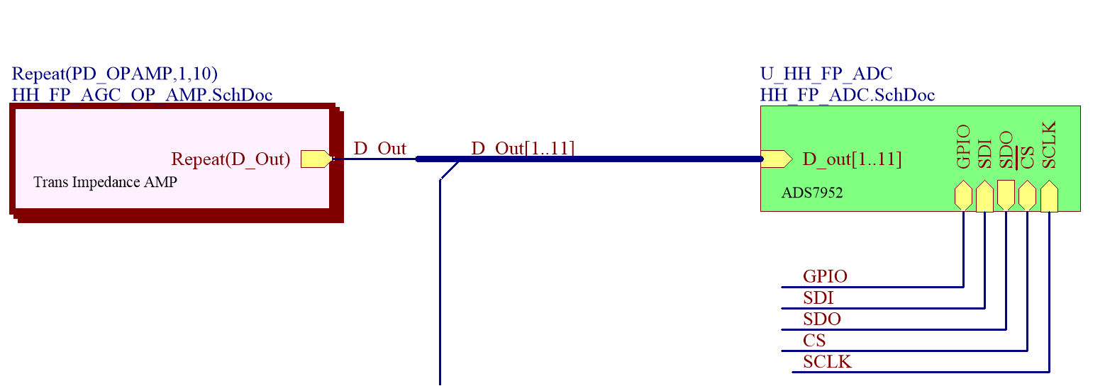
Top level file of my board

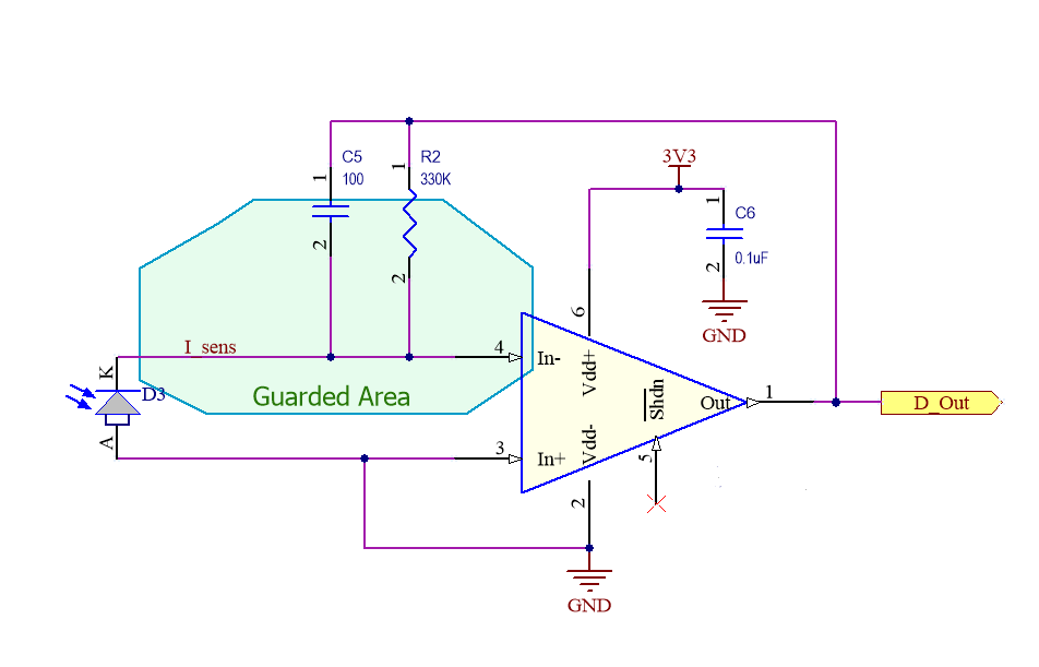
Trans-impedance amplifier

ADS7952


  • Hi Mirza,

    Thanks for providing detailed information in your query.

    Channel 8 of the MUX has nothing particular about it which is any different from the other MUX channels. Hence the glitches which you are observing on channel 8 seem to be an external interference.

    Could you please try the following two things -

    1) Could you wire the output of TIA driving channel 7 to channel 8 and vice versa. The expectation here is that, the glitches you are observing on channel 8 should now appear on channel 7.
    2) Could you please short the MUX channels 7 and 8 and drive them using the TIA driving channel 7 in your present schematic. Here, you can leave TIA which was driving channel 8 unconnected. This should yeild clean results on both channel 7 and channel 8.

    These two observations will help us understand the root cause of the problem.

    Your debug and analysis so far is very helpful. Thanks.

    Regards,
    Rahul
  • Hello

    I do not have possibility to switch the lines between channels as I am doing my debug on the PCB. I was able though to short ch7 and ch8. In addition to that I preformed some other test that I will discuss below:

    Tests:

    1.)    ALL INPUTS TO MUX FLOATING

    2.)    ALL INPUTS TO MUX FLOATING AND EXT VOLTAGE PRESENT BETWEEN MUX AND ADC

    3.)    CH8 FLOATING

    4.)    CH8 WITH EXT VOLTAGE

    5.)    CH7 AND CH8 SHORTED


    Results:

    1.)    ALL INPUTS TO MUX FLOATING

    The picture shows my setup. I left all the inputs to mux floating and shorted MUX->AINP. My scope probe was placed on the line between MUX and AINP.

    The purple line presents SSn and red line is SCL. The yellow line is the signal between MUX and AINP. I have zoomed the scope on the CH8. The 3rd SSn low is when CH8 is selected. As you can see on the previous 2 channels and 2 channels afterwards the signal is pretty clean in noiseless. When CH8 is selected noise is really high.

    2.)    ALL INPUTS TO MUX FLOATING AND EXT VOLTAGE PRESENT BETWEEN MUX AND ADC


    In this example I have left all the CH0-11 floating but on the line MUX->AINP I have connected a voltage source (RIGOL DP811A) with 55mV.


    The upper graph present all the channels read and I have zoomed only on CH8 (bottom graph). As you can see just with voltage between MUX and ADC, when CH8 is selected the noise is the greatest.


    3.)    CH8 FLOATING

    I connected all the channels to TIA except CH8 as show on the picture.

    The following picture shows the results. Again I have zoomed on the CH8 and you can see the noise popping up every transition on SCL.

    4.)    CH8 WITH EXT VOLTAGE

    Next I connected V-source to CH8 and set it to a) 0V and b) 55mV as depicted on following picture.

    Results of a) are presented on picture below.


    The fact that voltage is lower is expected as I have 0V on CH8 input. However the noise is completely unexpected and unacceptable.

    Next picture presents results when CH8 V-source is set to 55mV.


    What is surprising is that noise. This is when CH8 is connected to stable voltage source and once signal passes through MUX it gets so noisy.

    5.)    CH7 AND CH8 SHORTED

    As you have suggested I short connected CH7 and CH8 as shown on picture below. On my board I removed TIA from the PCB. I removed all the components of TIA OP amp and feedback components, so pin CH8 is sampling components of CH7.  


    This is the result. It is interesting to see that noise and offset has now spread to CH7.

  • Hello

    I do not have possibility to switch the lines between channels as I am doing my debug on the PCB. I was able though to short ch7 and ch8. In addition to that I preformed some other test that I will discuss below:

    Tests:

    1.)    ALL INPUTS TO MUX FLOATING

    2.)    ALL INPUTS TO MUX FLOATING AND EXT VOLTAGE PRESENT BETWEEN MUX AND ADC

    3.)    CH8 FLOATING

    4.)    CH8 WITH EXT VOLTAGE

    5.)    CH7 AND CH8 SHORTED


    Results:

    1.)    ALL INPUTS TO MUX FLOATING

    The picture shows my setup. I left all the inputs to mux floating and shorted MUX->AINP. My scope probe was placed on the line between MUX and AINP.


    The purple line presents SSn and red line is SCL. The yellow line is the signal between MUX and AINP. I have zoomed the scope on the CH8. The 3rd SSn low is when CH8 is selected. As you can see on the previous 2 channels and 2 channels afterwards the signal is pretty clean in noiseless. When CH8 is selected noise is really high.

    2.)    ALL INPUTS TO MUX FLOATING AND EXT VOLTAGE PRESENT BETWEEN MUX AND ADC

    In this example I have left all the CH0-11 floating but on the line MUX->AINP I have connected a voltage source (RIGOL DP811A) with 55mV.


    The upper graph present all the channels read and I have zoomed only on CH8 (bottom graph). As you can see just with voltage between MUX and ADC, when CH8 is selected the noise is the greatest.


    3.)    CH8 FLOATING

    I connected all the channels to TIA except CH8 as show on the picture.


    The following picture shows the results. Again I have zoomed on the CH8 and you can see the noise popping up every transition on SCL.


    4.)    CH8 WITH EXT VOLTAGE

    Next I connected V-source to CH8 and set it to a) 0V and b) 55mV as depicted on following picture.


    Results of a) are presented on picture below.


    The fact that voltage is lower is expected as I have 0V on CH8 input. However the noise is completely unexpected and unacceptable.

    Next picture presents results when CH8 V-source is set to 55mV.


    What is surprising is that noise. This is when CH8 is connected to stable voltage source and once signal passes through MUX it gets so noisy.

    5.)    CH7 AND CH8 SHORTED

    As you have suggested I short connected CH7 and CH8 as shown on picture below. On my board I removed TIA from the PCB. I removed all the components of TIA OP amp and feedback components, so pin CH8 is sampling components of CH7.  


    This is the result. It is interesting to see that noise and offset has now spread to CH7.

    Can you comment on these results?

    Thank you

  • Hi Mirza,

    Thanks for the detailed analysis.

    I think your experiments clearly point at a coupling between the digital activity and channel 8. At this stage we can rule out any coupling through the TIA.

    Could you please confirm the following -
    a) How many boards have you seen these observations on?
    b) Could you please share your schematic and layout PDFs? You could send it to rahulvk@ti.com
    c) Have you tried replacing the ADS7952 with another ADS7952 on this board?

    Thanks.

    Regards,
    Rahul
  • Hello

    thank you very much for your answer

    I will address your questions one by one:

    a) How many boards have you seen these observations on?


    I have build following:

    * 5 boards with LTC6268 ... they all work fine but current consumption is too high for our usage.

    * 3 boards with OPA314 ... they all show the same behavior as explained above

    * 3 boards with OPA320 ... they all show the same behavior as explained above

    * 1 board with OPA625 ... they show better behavior but still noise and offset on CH8 is noticeable and for our needs unacceptable 

    * 2 boards with no TIA just ADC ... same behavior as described above

    b) Could you please share your schematic and layout PDFs? You could send it to rahulvk@ti.com

    Please check your email box.

    c) Have you tried replacing the ADS7952 with another ADS7952 on this board?

    In all examples I explained under the first question i used new ADS7952.

  • Hi Mirza,

    Thanks for the update.
    I have sent my comments about the layout to your email box.

    Regards,
    Rahul
  • Hi

    Thank you very much for respecting my privacy and sharing the layout and the project.

    You have suggested to cut the trace to CH7 and connect it to CH6. Picture below.

    I have shorted CH6 and CH7 and cut the line to CH7. I left the CH8 connected to stable V-source as shown on picture above. The result is on the following picture.

    I think that this disproves our hypothesis. The CH6 and CH7 are very clean while CH8 is still noisy.

    I will also share how we control the ADC. As i have stated before we are running in manual mode.

    SSn MOSI (SDI) MISO (SDO)
    1 0x1800 0x1xxx
    2 0x1880 0x2xxx
    3 0x1900 0x0xxx
    4 0x1980 0x1xxx
    5 0x1A00 0x2xxx
    6 0x1A80 0x3xxx
    7 0x1B00 0x4xxx
    8 0x1B80 0x5xxx
    9 0x1C00 0x6xxx
    10 0x1C80 0x7xxx
    11 0x1D00 0x8xxx
    12 0x1D80 0x9xxx
    13 0x1800 0xAxxx
    14 0x1880 0xBxxx
    15 0x1900 0x0xxx

    Do you have any thoughts?

    Thank you

  • Hi Mirza,

    I have replied to your query via email.

    Please check you mail box.

    Thanks.

  • Hi Mirza,

    I am closing this thread and summarizing our offline conversation.

    The coupling was happening due to channel 8 and SCLK trace running parallel to each other without an intermediate ground layer.
    This was confirmed by making an engineering board where the digital traces were kept away from the analog traces. On this engineering board, the channels were seen to be clean.

    Thanks for evaluating the debug steps and going the extra mile in providing the additional info which helped us narrow down to the problem location.