This thread has been locked.

If you have a related question, please click the "Ask a related question" button in the top right corner. The newly created question will be automatically linked to this question.

ADS1198: ADS1198 data extraction

Part Number: ADS1198

Hai

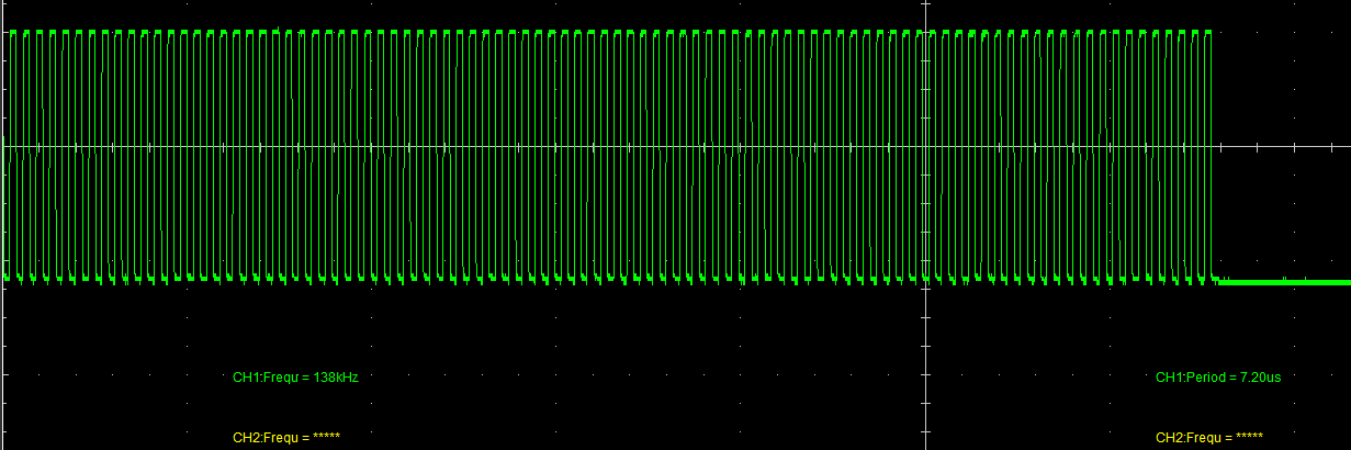
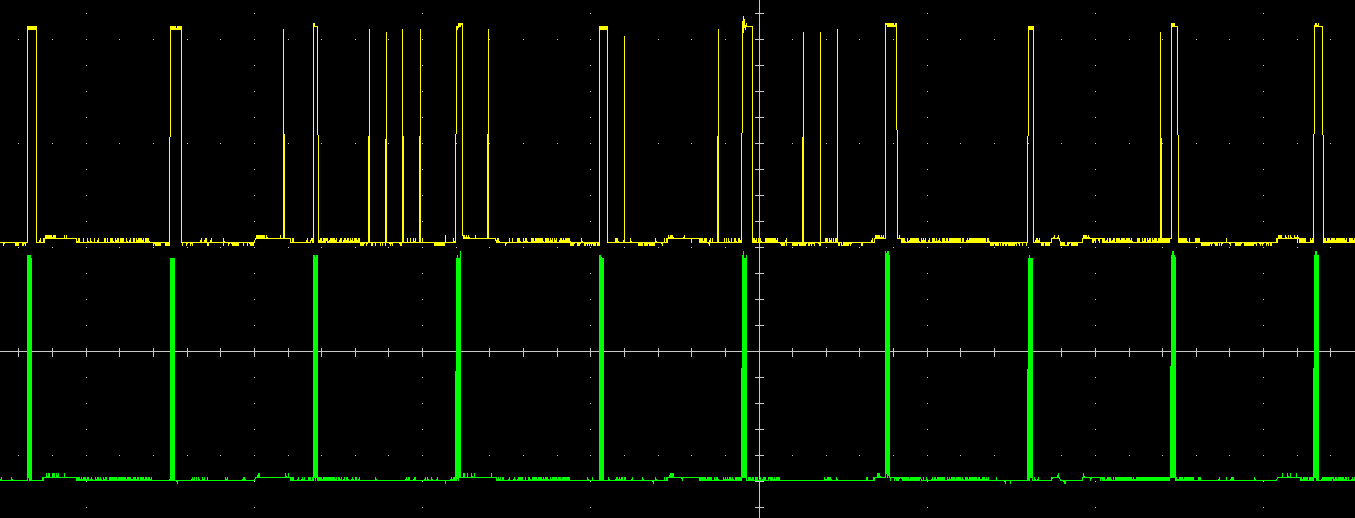
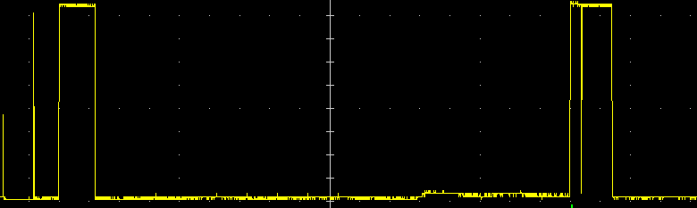
I am currently working on the project with ADS1198 and STM32F103RCT6 controller.The project is completed upto spi data transfer,With the help of ECG simulator I am able to receive 19 byte data out.

In the datasheet  it is mentioned that the data is in the 2's complement format with MSB first. Can anyone please help me to tell how the data is extracted?

  • Hello Silpa,

    The data is retireved via the SPI interface. When the device is configured in RDATAC mode, the host can simple wait for a DRDY negative edge, then pull CS low and begin toggling SCLK. The device will automatically shift out conversion data on the DOUT pin. You should toggle SCLK enough times to shift out the 24-bit status word and 8 channels worth of 18-bit conversion data - a total of 168 bits each time DRDY transitions low. There are details about data retrieval and other aspects of the SPI interface in the ADS1198 datasheet which you can find here: www.ti.com/.../ads1198.pdf

    Regards,
    Brian Pisani
  • Hai Sir

    Thanks for the reply.In the reply you mentioned about the 168 bits ,Are you sure about that? According to ADS1198 data sheet ,it consist of 8 channels of 16 bits each and consist of 24 status bits so total of 152 bits,Isn't it?

     I have successfully outed the 19 byte data via Spi.I am using an ECG simulator to give the input signals.My current issue is :

    1)How to separate the data for each channel from that 19 byte data stream? 

    2)For plotting the data I want to convert this 2's complement data to signed integer,right?

  • Silpa,

    Yes you are correct about the number of bits. My math was wrong.

    1. You will need to write some code to perform the logic operations required to separate out the channels. I do not have any sample code, but it shouldn't be too difficult. It will mostly consist of masking off unnecessary bits and bit shifting to get the words properly aligned.
    2. Yes you will probably have to get the data into a signed format. I do not know exactly how your processor works (word size/types, etc.), but given that the data you are getting will be 16 bits wide, there should be some data type that fits easily to the data where you could use a cast to change how it is stored. For example, the data type "signed short" typically corresponds to a 2's complement, signed, 16 bit integer. Otherwise, "int16_t" is pretty universal in c to correspond with that type.

    Regards,

    Brian Pisani

  • Hello Sir 

    Thanks for the previous reply.I have one new doubt,for ADS1198 i shutdown all the 8 channel by setting up of the register, so  the values should be '0'for all channels,but at sometimes, for some channel it outputs  some junk values like ( C0 00 00 00 00 00 00 00 00 00 00 00 00 00 1C 00 00 00 00 ).What may be the reason for this? how can i solve this?

  • Silpa,

    Check the SPI signals on the logic analyzer. It could be that you are not reading the entire data transfer before the next DRDY signal occurs. To see this, look at SCLK, DRDY, and DOUT to see what is happening when the bad read occurs.

    Brian
  • Sir

    I am working on this for the last one month ,still when i plot the waves ,it just look like the noise.I have encounter many problems with this ,i will mention it below 

    1) In the datasheet of ADS1198 in the timing characteristics there it gives the SPI settings as CPOL=1 and CPHA=1, but for my ADS1198 i am getting the dataout only when CPOL=1 and CPHA=2.

    2)when i gone through the TI forum ,you suggest some person to check the AVDD,AVSS etc so i also checked for my circuit,That i will mention below

    • AVDD=2.4V
    • AVSS=0
    • DVDD=2.4V
    • VCAP1=1.18V
    • VCAP2=1.22V
    • VCAP3=4.27V
    • VCAP4=1.1V

    I am using supply of 3.3v and internal reference 2.4v

    3)My programming flow is like 

    •  call ADS reset function (in that i will reset and set the reset pin,then reset the chip select)
    • ADS stop conversion
    • ADS SDATAC
    • then register write and read
    • send ADS start opcode

    but when i viewed the DRDY pin i am getting a high to low pulse. i am attaching the files below

    this is the sclk ,for the normal default condition min sclk is 80khz ,i am also following the default condtion as and using spi sclk as 138,nearly 140kHz

    The above picture shows Dout(yellow) and Sclk(green) 

    The above picture shows the DRDY (yellow) and sclk(green).

    4) C0 00 00 00 00 21 80 00 00 00 00 42 0A 00 00 00 00 00 00    C0 00 00 00 00 21 D7 00 00 00 00 00 00 0C 00 00 00 00 02.

    above i have shown a 2 Dout patterns with C0 header ,here i have opened only 2nd channel and shutdown all other channel still the output looks like this.

    these are my current issue, I don't know how to solve this , please help me as fast as possible ,i am stuck with this situation. 

  • Hello Silpa,

    I can't tell what is going on in any of those images. Could you zoom in on a single transaction (i.e. when DRDY comes low and what happens immediately afterwards)? I'd like to see DRDY, SCLK, and DOUT.

    The voltage AVDD - AVSS must be at least 2.7 V for the device to work properly. If this is not the case, you cannot expect the device to work.

    Brian
  • Sir

    Thanks for the reply ,i can understand your difficulty ,but my problem is i am using a PC oscilloscope ,with that i am not able to check the waveform precisely.

    I tired to view the sclk but still it is not  able to view it properly,so currently i may not be able to zoom the single transactions.

    can you please clarify some of my doubts?

    this is my DRDY. Is this waveform correct? Normally it should be a high pulse when data becomes ready it become low ,right? what may be the reason for this inversion in the above waveform?

    I have one more ADS board,so i checked the parameter values ,can you please verify it please?

    • AVDD=3.5V
    • AVSS=0V
    • DVDD=3.3V
    • VCAP1=1.29V
    • VCAP2=1.7V
    • VCAP3=5.4V
    • VCAP4=0.5V 

  • Silpa,

    The power supply and VCAP values look correct, except for VCAP4. VCAP4 should be equal to VREFP/2. What is the voltage at VREFP? Have you been able to successfully write the register which enables the internal reference buffer?

    My best guess at this point is that this issue you are seeing is related to the way you are communicating with the SPI interface. Unfortunately it is extremely difficult to debug interface issues without access to a proper oscilloscope or logic analyzer. Do you have access to a lab that has one? Could you borrow one from a friend or colleague?

    Brian
  • Sir

    I am using 2.4 v internal reference as my reference voltage .I have already enabled it by setting bit5=0 of the config3 register.And about the oscilloscope ,i am not sure about it ,i will try my level best to get a proper oscilloscope .Thanks for you help.