This thread has been locked.

If you have a related question, please click the "Ask a related question" button in the top right corner. The newly created question will be automatically linked to this question.

DAC3484: DAC3484 output harmonics with a sine wave input

Part Number: DAC3484

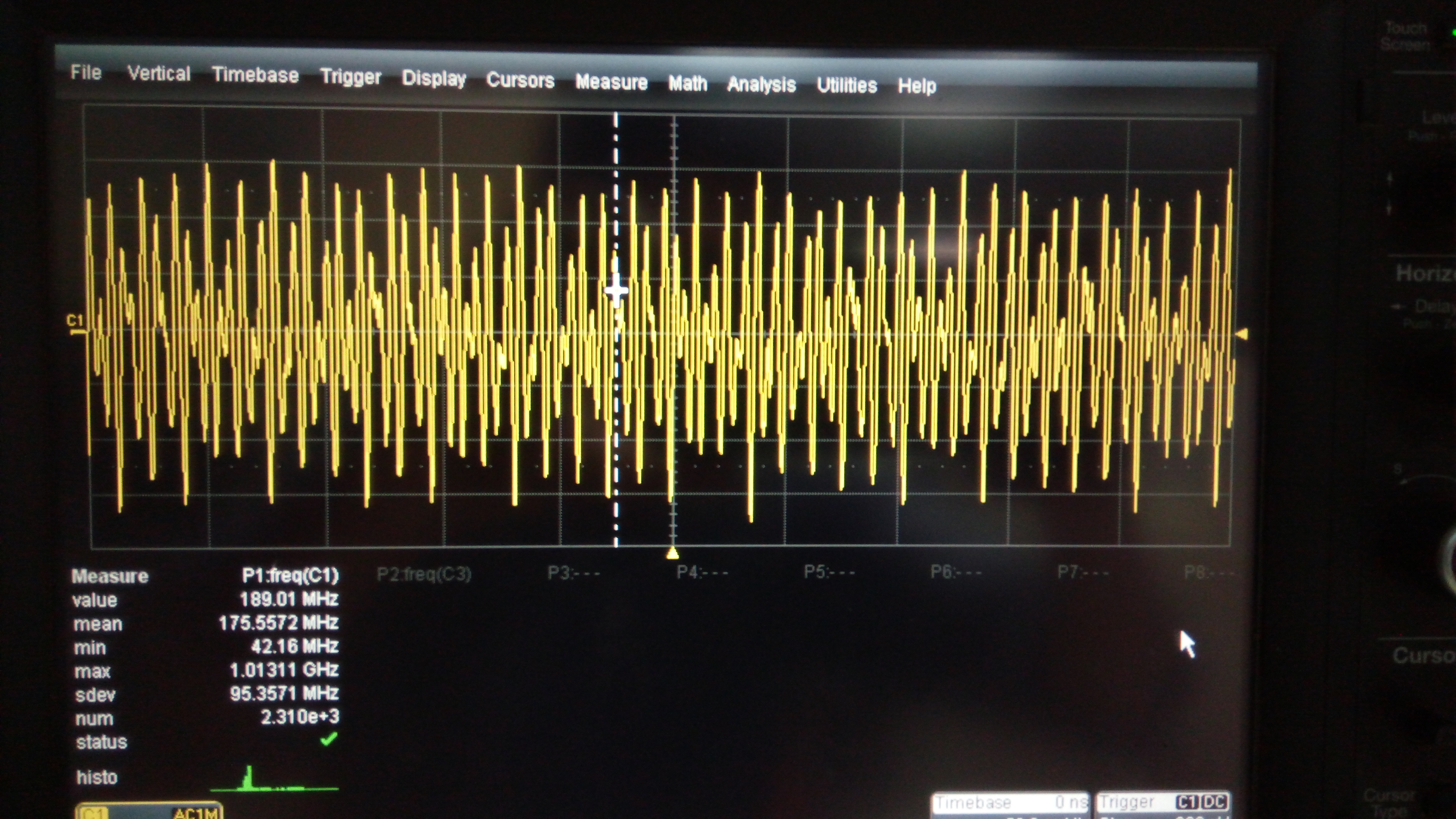
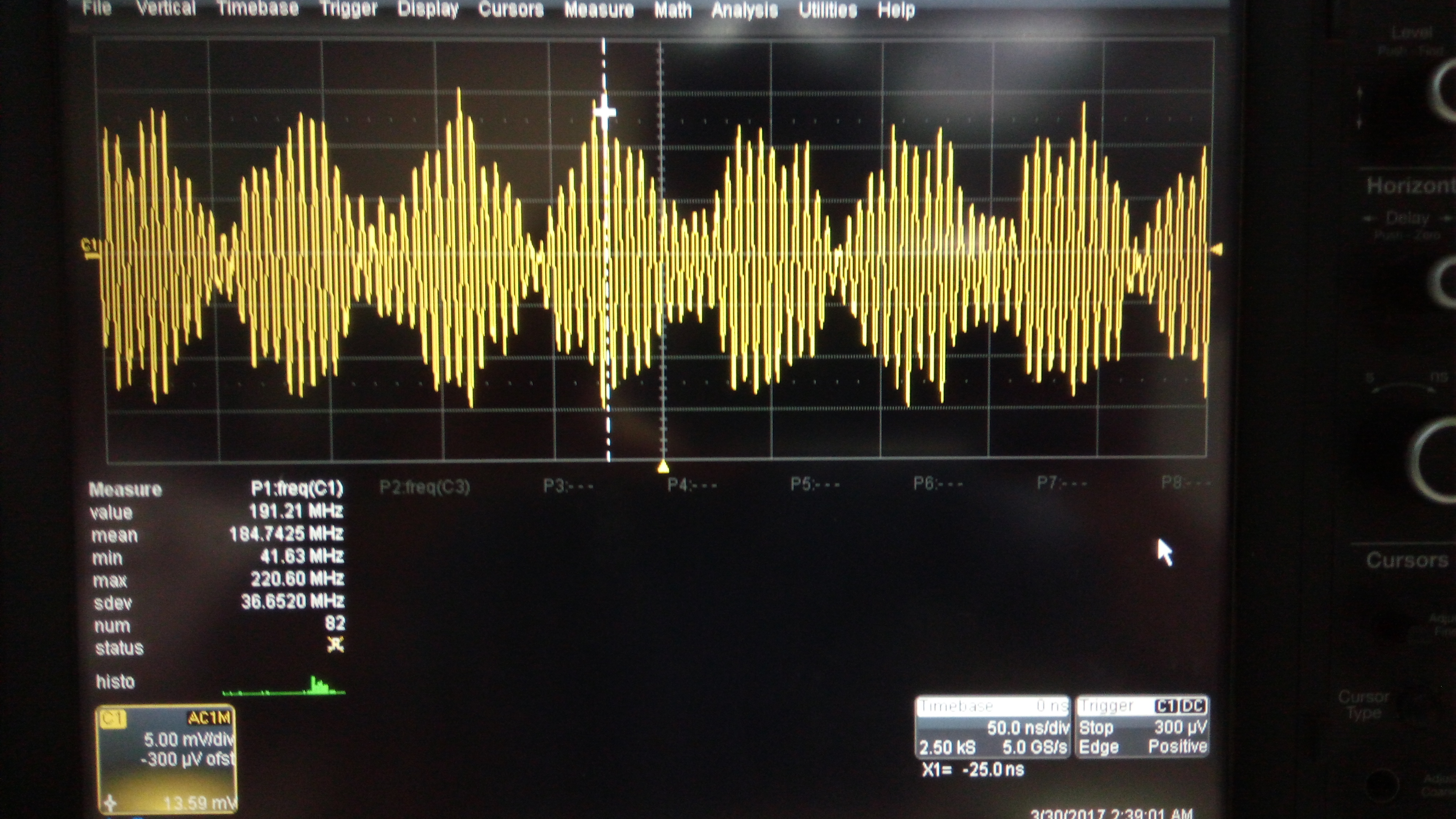
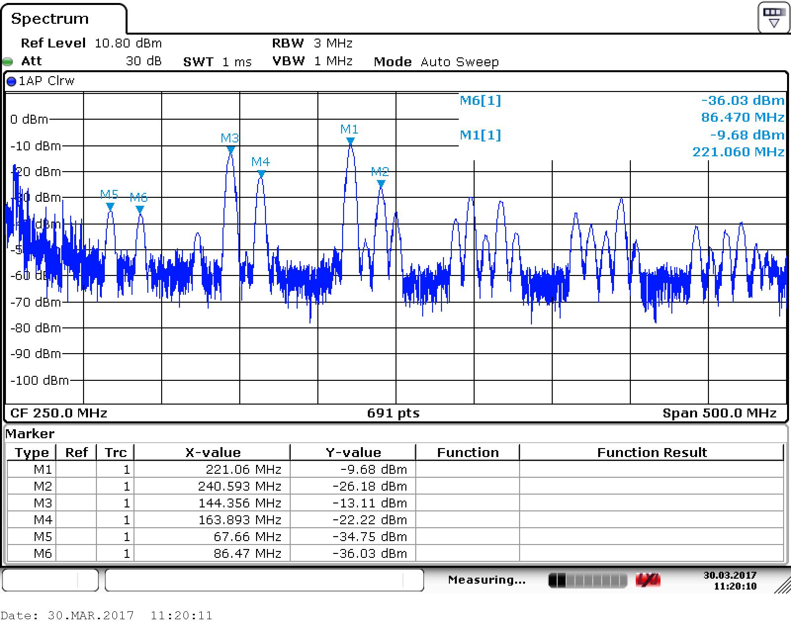
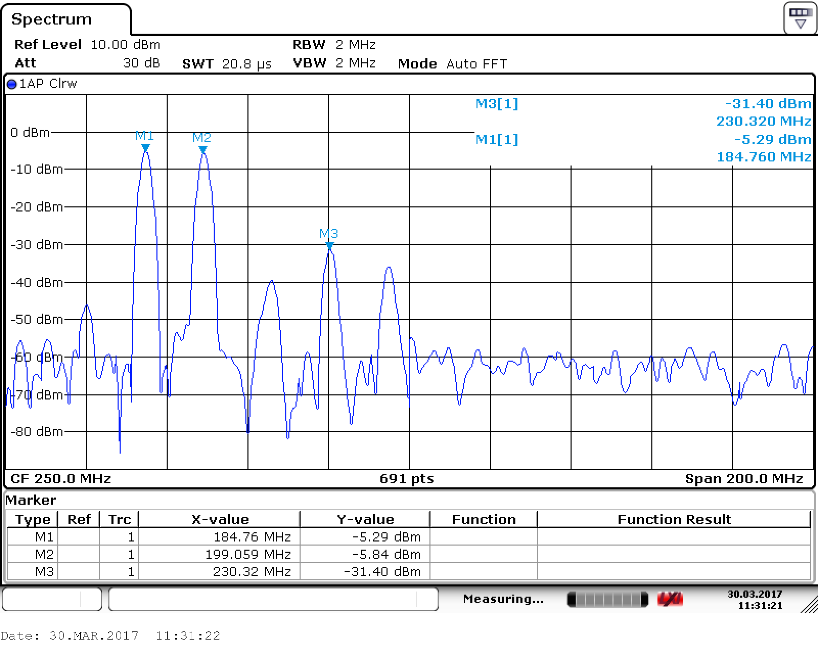
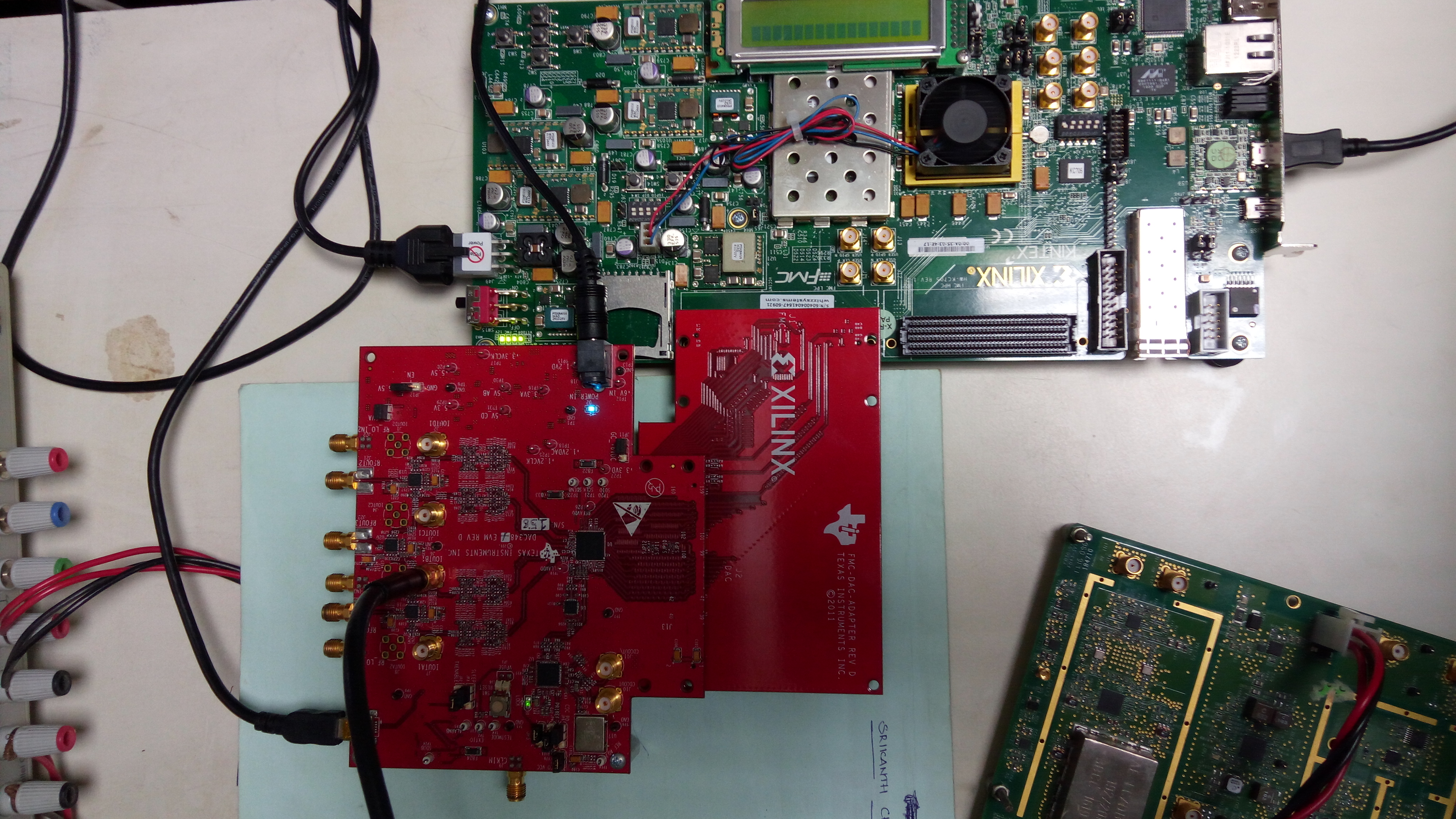
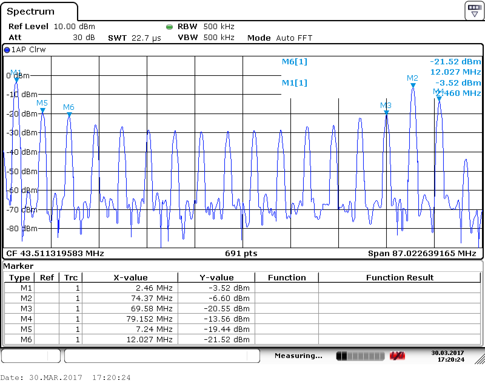
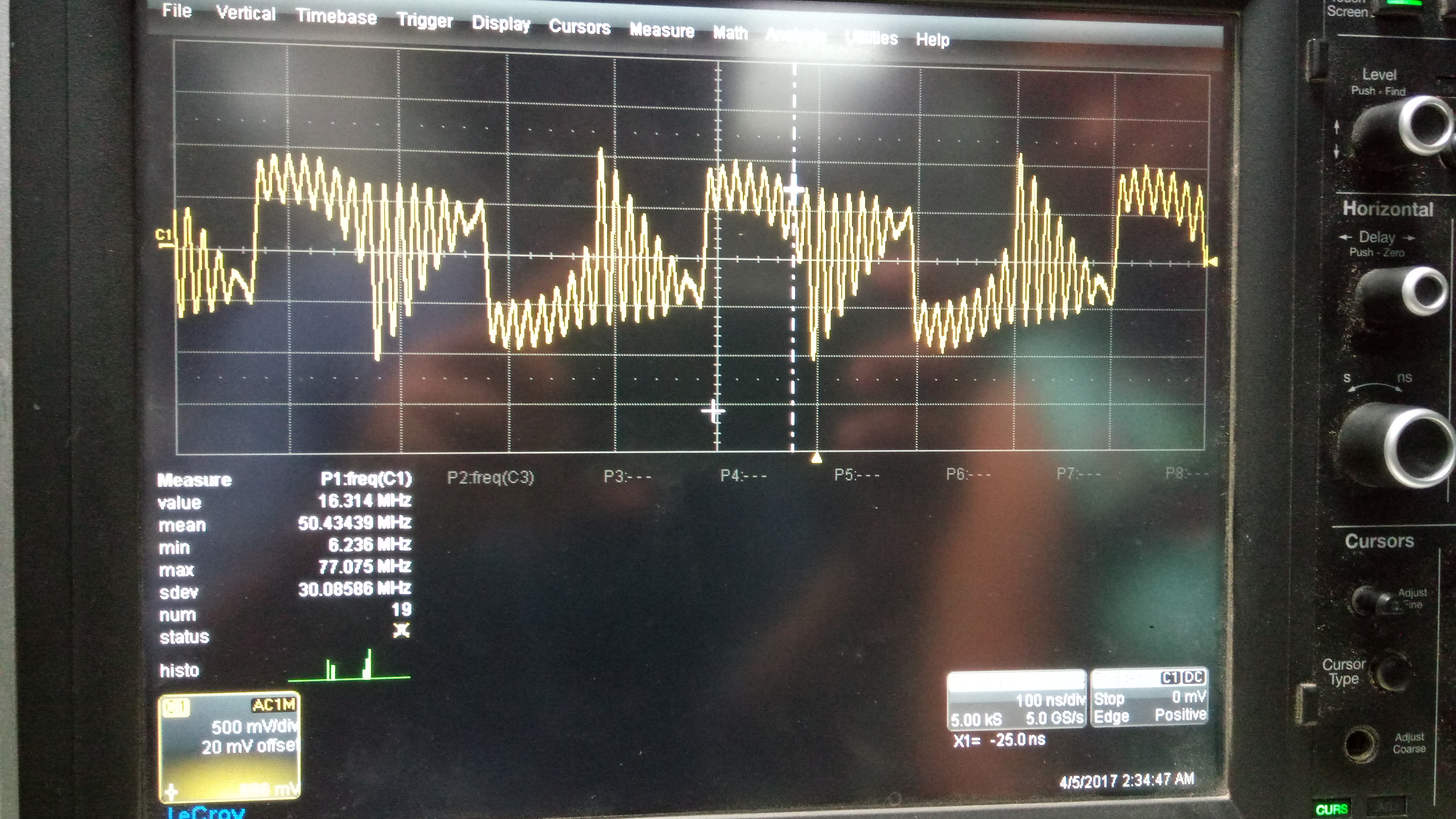
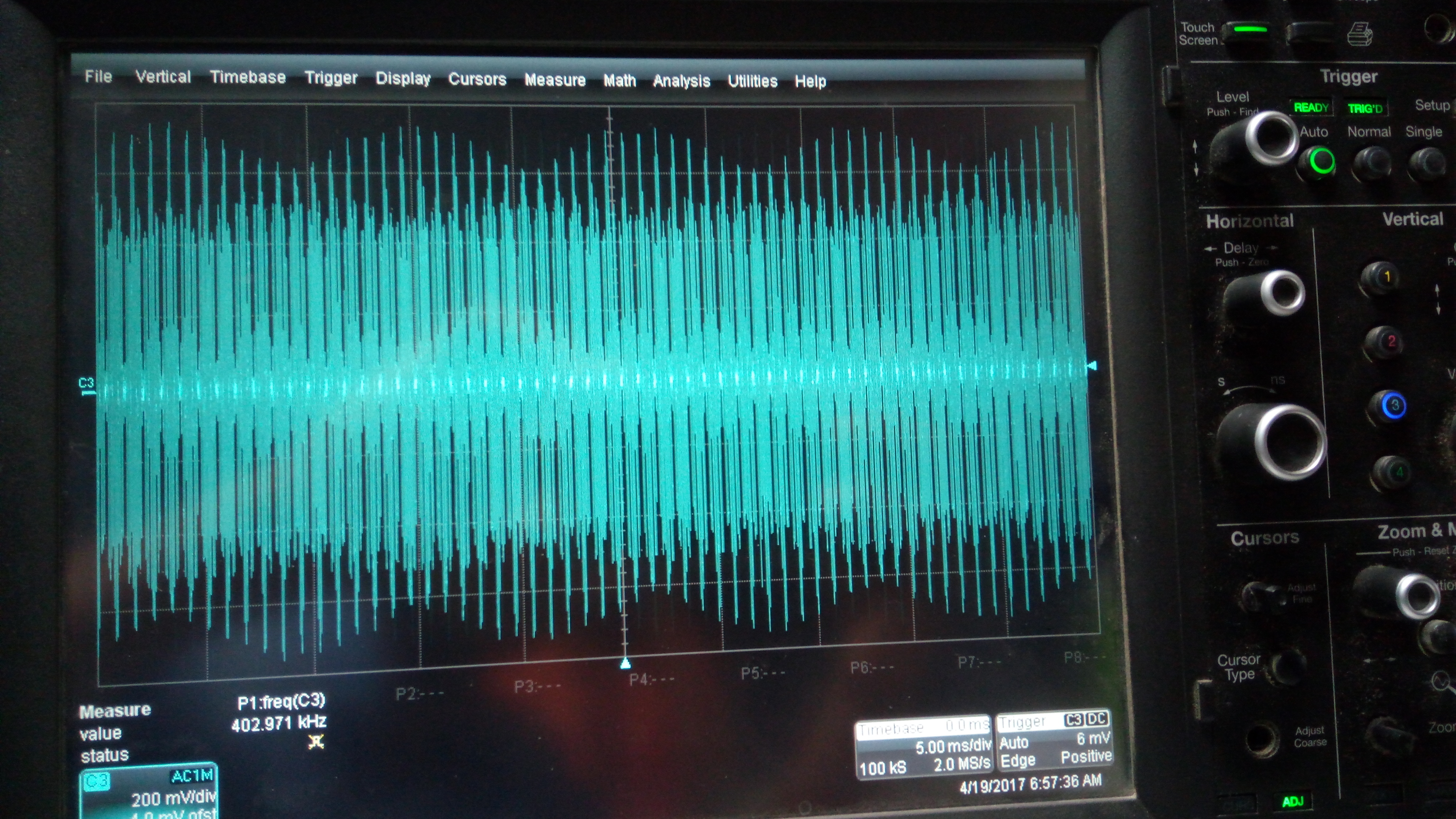
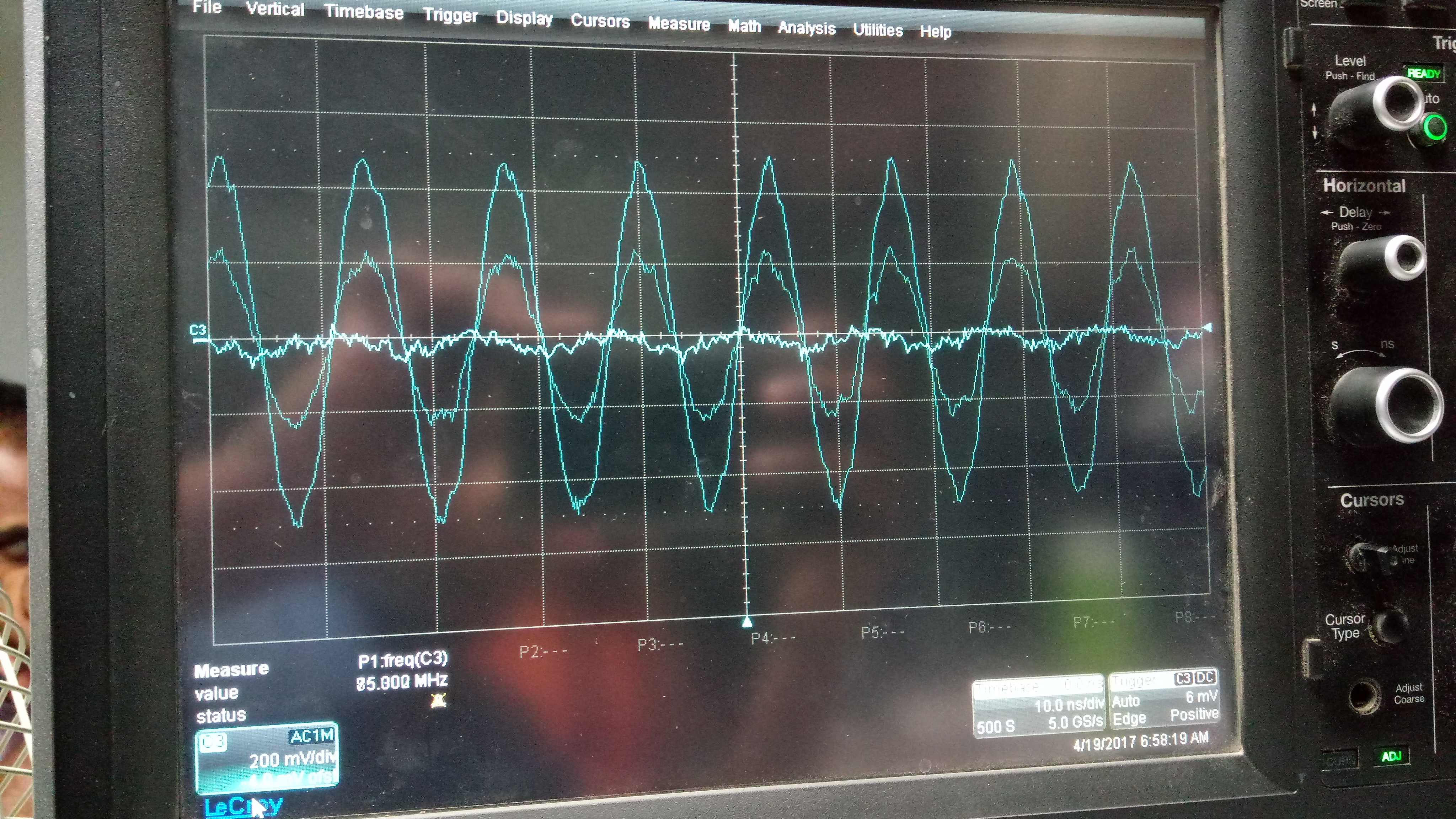
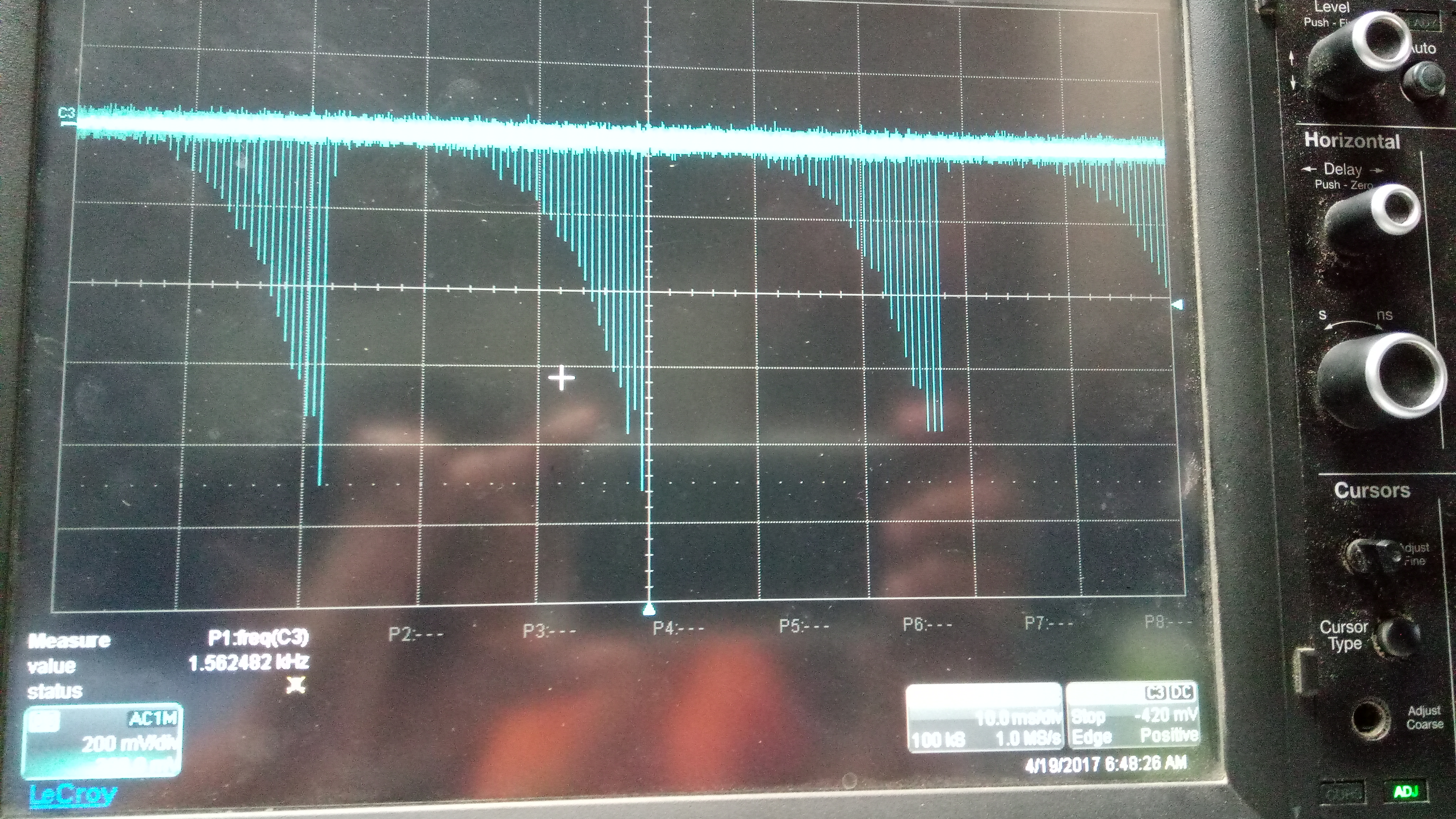
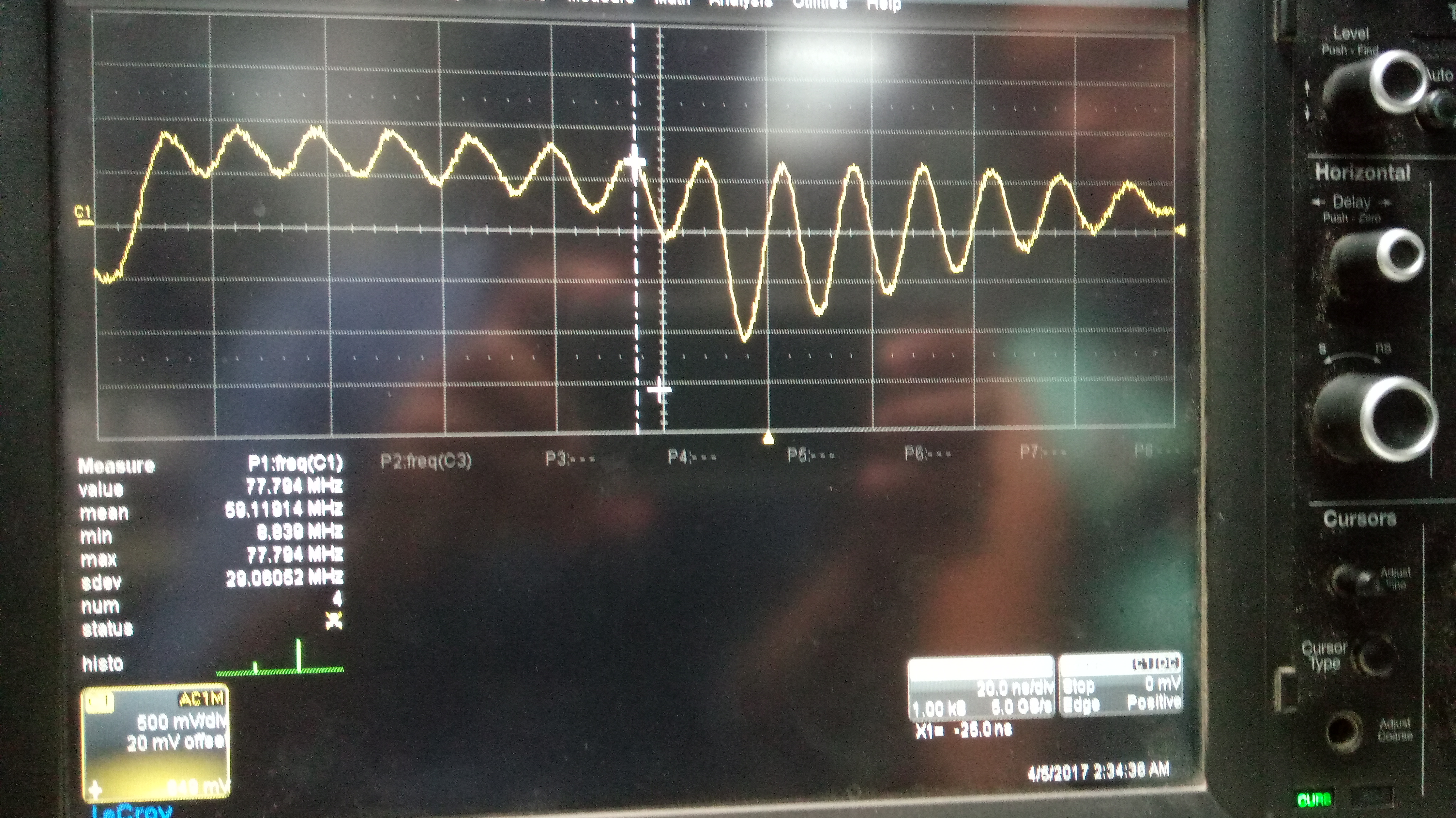
          We have designed a platform in which DAC3484 is interfaced with xilinx FPGA through FMC-HPC. Here, we tried giving 7MHz sine wave to all four four channels (I0 Q0 I1 Q1) generated from DDS in FPGA at 153.6MSPS rate.

The DACDATA_CLK is 307.2 and DAC_CLK is 614.4 (interpolation by 4). the DAC NCO is configured for 192MHz. FRAME signal has used for syncing source for FIFO. and NCO sync source is SIFSYNC.

but we had observed that there are two harmonics at 199MHz (192+7) and 185MHz (192-7) on the DAC output of channel C-D and 199MHZ on channel A-B. 

what could be reason for such behavior ? 

The reguster setting is given below,

Cw0 <= x"00_028F";
Cw1 <= x"01_0100";
Cw2 <= x"02_80D2"; -- mixer gain disabled
Cw3 <= x"03_D000";
Cw4 <= x"04_0000";
Cw5 <= x"05_0000";
Cw6 <= x"06_3300";
Cw7 <= x"07_FFFF";
Cw8 <= x"08_0000";
Cw9 <= x"09_8000";
Cw10 <= x"0A_0000";
Cw11 <= x"0B_0000";
Cw12 <= x"0C_0400";
Cw13 <= x"0D_0400";
Cw14 <= x"0E_0400";
Cw15 <= x"0F_0400";
Cw16 <= x"10_0000";
Cw17 <= x"11_0000";
Cw18 <= x"12_0000";
Cw19 <= x"13_0000";
Cw20 <= x"14_0000";--- reg 0x14-0x17 IF=192MHz
Cw21 <= x"15_5000";
Cw22 <= x"16_0000";
Cw23 <= x"17_5000";
Cw24 <= x"18_2000";
Cw25 <= x"19_0000";
Cw26 <= x"1A_0020";
Cw27 <= x"1B_0800";
Cw28 <= x"1C_0000";
Cw29 <= x"1D_0000";
Cw30 <= x"1E_1111";
Cw31 <= x"1F_8880";
Cw32 <= x"20_2201";
Cw34 <= x"22_1B1B";
Cw35 <= x"23_FFFF";
Cw36 <= x"24_1800";
Cw37 <= x"25_7A7A";
Cw38 <= x"26_B6B6";
Cw39 <= x"27_EAEA";
Cw40 <= x"28_4545";
Cw41 <= x"29_1A1A";
Cw42 <= x"2A_1616";
Cw43 <= x"2B_AAAA";
Cw44 <= x"2C_C6C6";
Cw45 <= x"2D_0004";-
Cw46 <= x"2E_0000";
Cw47 <= x"2F_0000";
Cw48 <= x"30_7FFF";

  • Hi,

    Are you sending in complex signal into the AB and CD channels?  in other words sine and cosine at 7MHz?

    The NCO mixer is a complex mixer, if the input signal is sin on both A and B, then it is treated as a real signal and the sideband signal will not cancel.  The signal will then appear as a real signal at the NCO frequency (double sideband around the NCO).  If the signal is complex (single sideband) then the signal will appear at the outputs on only 1 side of the NCO frequency (one of the sidebands will cancel in the complex mixer).

    Please confirm if you are sending a complex signal into AB and CD.

    Ken

  • Hi,

    We are still seeing the same issues, we are giving samples from two DDS blocks generated in kintex-7 FPGA
    (one 7.199MHz to cahnnel A and B and 9.599Mhz to channel C and D), as Sine to channel A and Cosine to channel B and also for channel C and D respectively.

    DAC configuration-
    DACDATACLK – 307.2MSPS
    DACCLK – 614.4MSPS
    DAC NCO – 192MHz
    Interpolation – 4x
    syncsel_mixerAB=sif_sync
    syncsel_mixerCD=sif_sync
    syncsel_NCO=sif_sync
    syncsel_dataformatter=FRAME
    syncsel_fifoin = Frame
    syncsel_fifoout = Frame
    sequence followed:
    1) DAC reset
    2) program DAC registers
    3) provide sif sync
    4)generated an internal signal flag=1
    5)upon flag=1, after certain delay OSERDES(output serializer deserializer primitives, used for muxing channel A,B,C,D data at 153.6MHz rate to 307.2MHz clock as required by DAC) blocks in FPGA are reset and enabled

    6) FRAME pulse is generated
    7) DAC Txenable pulled high

    Two DDS are used to generate IQ (sine and cosine) for both DAC channels separately with frequencies mentioned above. The output rate is 153.6MSPS and DAC dataclk of 307.2MSPS.

    We found two components at 199.2MHz (192+7.2) and 184.8 MHz (192-7.2) in I1 and Q1 out. The same has noticed in I2 and Q2 out also. and upon powering OFF and ON analog card (where DAC3484 is placed) keeping Digital card (Where FPGA is placed) powered ON, we have seen components were at 182.4MHz (192-9.6) and 201.6MHz (192+9.6) respectively and which has changed to 199.2MHz (192+7.2) and 184.8 MHz (192-7.2) upon RESETing FPGA.
  • Hi ken,

    We are sending complex signal from Kintex-7 FPGA. we have generated two DDS compilers, one 7.199MHz and other 9.599MHz. we are sending sine to channel A and Cosine to channel B (7.199MHz) and also for channel C and D respectively (9.599MHz).

    The configurations are given below,

    DAC configuration-
    DACDATACLK – 307.2MSPS
    DACCLK – 614.4MSPS
    DAC NCO – 192MHz
    Interpolation – 4x
    syncsel_mixerAB=sif_sync
    syncsel_mixerCD=sif_sync
    syncsel_NCO=sif_sync
    syncsel_dataformatter=FRAME
    syncsel_fifoin = Frame
    syncsel_fifoout = Frame

    sequence followed:
    1) DAC reset
    2) program DAC registers
    3) provide sif sync
    4)generated an internal signal flag=1
    5)upon flag=1, after certain delay OSERDES(output serializer deserializer primitives, used for muxing channel A,B,C,D data at 153.6MHz rate to 307.2MHz clock as required by DAC) blocks in FPGA are reset and enabled
    6) FRAME pulse is generated
    7) DAC Txenable pulled high

    Two DDS are used to generate IQ (sine and cosine) for both DAC channels separately with frequencies mentioned above. The output rate is 153.6MSPS and DAC dataclk of 307.2MSPS.

    We first configure the FPGA and given a RESET which interns configures DAC and digital samples will be provided from the DDS to DAC. After giving RESET to FPGA, We found two components at 199.2MHz (192+7.2) and 184.8 MHz (192-7.2) I1 and Q1 out . The same has noticed in I2 and Q2 out also.
    Then we powered OFF and ON the analog card (where DAC3484 has placed) keeping FPGA powered ON we have seen frequency components at 182.4MHz (192-9.6) and 201.6MHz (192+9.6) respectively.
    Upon giving FPGA RESET the spectrum has changed to 199.2MHz (192+7.2) and 184.8 MHz (192-7.2) for both channels.

    Regards,
    Nandakumar CM
  • Hello,
    Please help closing this.
  • Hi,

    Can you please do a couple of experiments.

    Turn off the NCO in the DAC and monitor the output of A, B , C, D.

    if you look at A and B you should see sine and cosine 7.2M - please monitor both outputs on a scope and ensure that they are sine/cos with 90 degree offset.  Do the same for C and D outputs you should see 9.6M sin/cos with 90 degree offset.

    If you do not see this then the data is not getting into the DAC correctly.

    Please confirm that you see this without the NCO 1st.

    Ken

  • Dear Ken C,

    we had tried all pattern check. we found that all the pattern checks were fine hence the data interface seems to be okay.
    we had tried both single frame pulse and periodic frame also. so does it imply --- the data interface and data transfer between FPGA and DAC3484 is fine?

    and we tried disabling DAC NCO and we found some spurious at different higher frequencies and we did not find any DAC output when we tried disabling mixer_enable too.

    So we are not sure about the cause of the issue and what can we conclude on the basis of pattern check? is that the only way to check the data interface ? so one basis of pattern check results, does it mean that our data interface and FRAME generation is fine?

    regards,
    Nandakumar

  • Please send a screen shot of channels A and B with the NCO mixer set to OFF.  If you do not see a sine or cosine, then your interface may not be working correctly, or your digital format (offset binary or 2s complement) may not be aligned between the FPGA and DAC.

    A screen shot of the DAC output would help us understand the possible issue.

    The other thing to try is to set the DAC input to constant level such as 0000 and then setting the input format to offset binary (this is in the INPUT Tab and is basically fullscale DC), then enable the NCO which will modulate the input DC level to the NCO frequency.  You should be able to measure a sine and cosine at the NCO frequency on output A and B.

    If this works then that means the DAC Is configured correctly and the NCO is working properly and the problem is in your digital interface/signal.

    Ken


  • Dear ken,

    please find the attached screenshots.

    DAC outputs when NCO disabled.

    .

    DAC outputs when NCO is enabled.

    The analyser plots.

    when NCO disabled.

    and when NCO is enabled.

     tgh

    The DC input was giving a single tone output at NCO frequency (192MHz). 

    we tried with the DAC3484 evaluation module aslo ,  kintex7 fpga evaluation module is used for data interface.  DAC was configured using evaluation software. 

    We have given 2.4 MHZ sinusoidal IQ and the plots were taken with NCO and MIxers disabled.

  • You mention that with DC input the outputs are at the NCO frequency with sine on A and cos on B. If this is true, this means the DAC is working fine.

    If you turn off the NCO and cannot get the DAC to output the correct signal, then that means you may have interface problems between the FPGA and DAC input.

    Can you send a time domain plot (oscope) of the last spectral plot showing the 2.4MHz signal?

    Ken.
  • We had given 2.4MHz sine wave from kintex7 eval board to DAC484 EVM. The DAC NCO and mixer are disabled.

  •       This is the dac data interface written for KC705 and DAC3484 eval board setup. By 
    changing the mode attribute (C_DAC_MODE ) same code works for self test, pattern check, sine test 
    and actual data. Self test and Pattern check worked fine with this code. Two of the 
    dac lines were inverting (line 3 and line 12) on pcb due to some issue. So these two 
    lines were purposefully inverted in the code so that final one is correct. Plz check 
    the data interface and let us know if you find some issue in the logic. 

    library IEEE;
    use IEEE.STD_LOGIC_1164.ALL;
    library UNISIM;
    use UNISIM.VComponents.all;
    use IEEE.STD_LOGIC_ARITH.ALL;

    entity dac_datainterface is
    generic (
            C_DAC_MODE                  : integer range 0 to 3:= 2
                                        -- 0 self test
                                                          -- 1 is fixed pattern mode
                                        -- 2 is sine wave mode
                                        -- 3 is actual data mode
             );

        Port (
                        mmcm_locked : in std_logic;
               DAC_CLK : in STD_LOGIC; --- f= 2*data rate of dac input
               DAC_CLKby2 : in std_logic; -- f= data rate of dac input (each channel)
               DAC_I1 : in STD_LOGIC_VECTOR (15 downto 0); --- f= data rate of dac input
               DAC_Q1 : in STD_LOGIC_VECTOR (15 downto 0);
               DAC_I2 : in STD_LOGIC_VECTOR (15 downto 0);
               DAC_Q2 : in STD_LOGIC_VECTOR (15 downto 0);
              
               DAC_DATACLK_P : out STD_LOGIC; --f= 2*data rate of dac input
               DAC_DATACLK_N : out STD_LOGIC;
               DAC_FRAME_P : out STD_LOGIC;
               DAC_FRAME_N : out STD_LOGIC;
               DAC_SYNC_P : out STD_LOGIC;
               DAC_SYNC_N : out STD_LOGIC;
               DAC_DATA_P : out STD_LOGIC_VECTOR (15 downto 0);
               DAC_DATA_N : out STD_LOGIC_VECTOR (15 downto 0)         
               );
    end dac_datainterface;

    architecture Behavioral of dac_datainterface is

    COMPONENT sine_wave_gen
      PORT (
        aclk : IN STD_LOGIC;
        m_axis_data_tvalid : OUT STD_LOGIC;
        m_axis_data_tdata : OUT STD_LOGIC_VECTOR(31 DOWNTO 0)
      );
    END COMPONENT;
    COMPONENT sine_wave_gen_1
      PORT (
        aclk : IN STD_LOGIC;
        m_axis_data_tvalid : OUT STD_LOGIC;
        m_axis_data_tdata : OUT STD_LOGIC_VECTOR(31 DOWNTO 0)
      );
    END COMPONENT;

    signal dac_dataclk_prebuf,dac_frame_i,dac_frame_prebuf,io_rst,m_axis_data_tvalid,m_axis_data_tvalid1: std_logic;
    signal DAC_I1_i,DAC_Q1_i,DAC_I2_i,DAC_Q2_i,dac_data_prebuf,DAC_corrected_I1,DAC_corrected_Q1,DAC_corrected_I2,DAC_corrected_Q2 : STD_LOGIC_VECTOR (15 downto 0);
    signal m_axis_data_tdata,m_axis_data_tdata1 :STD_LOGIC_VECTOR(31 DOWNTO 0);

    signal DAC_samp0,DAC_samp1,DAC_samp2,DAC_samp3,DAC_samp4,DAC_samp5,DAC_samp6,DAC_samp7 : STD_LOGIC_VECTOR (15 downto 0);

    signal dac_sync_prebuf : std_logic;

    begin
    ---------------DAC data source sel, data mux, frame generation-------------------------

    dacdatamux_selftest: if C_DAC_MODE = 0 generate
    begin
    ----in self test dac data and frame does not bother. dac dataclk needs to be running----
            DAC_samp0 <= x"00ff" ;
          DAC_samp1 <= x"00ff" ;
          DAC_samp2 <= x"00ff" ;
          DAC_samp3 <= x"00ff" ;
         
          DAC_samp4 <= x"00ff" ;
          DAC_samp5 <= x"00ff" ;
          DAC_samp6 <= x"00ff" ;
          DAC_samp7 <= x"00ff" ;

    end generate;
         
    dacdatamux_fixedpattern: if C_DAC_MODE = 1 generate
    begin
          DAC_samp0 <= x"7a7b" ;
          DAC_samp1 <= x"b6b6" ;
          DAC_samp2 <= x"eaea" ;
          DAC_samp3 <= x"4545" ;
         
          DAC_samp4 <= x"1a1a" ;
          DAC_samp5 <= x"1616" ;
          DAC_samp6 <= x"aaaa" ;
          DAC_samp7 <= x"c6c6" ;

    end generate;

    DAC_SINETEST :if C_DAC_MODE = 2 generate
    begin

    DAC_SINE_WAVE_GEN : SINE_WAVE_GEN --around 2.4MHz
      PORT MAP (
        aclk => DAC_CLKby2,
        m_axis_data_tvalid => m_axis_data_tvalid,
        m_axis_data_tdata => m_axis_data_tdata
      );

    DAC_SINE_WAVE_GEN1 : SINE_WAVE_GEN_1 --around 7.2MHz
      PORT MAP (
        aclk => DAC_CLKby2,
        m_axis_data_tvalid => m_axis_data_tvalid1,
        m_axis_data_tdata => m_axis_data_tdata1
      ); 
            DAC_samp0 <= m_axis_data_tdata1(31 downto 16);  --ChA Q2
            DAC_samp1 <= m_axis_data_tdata1(15 downto 0);  --ChB I2
            DAC_samp2 <= m_axis_data_tdata(31 downto 16);  --ChC Q1
            DAC_samp3 <= m_axis_data_tdata(15 downto 0); --sine --ChD I1
           
            --- samp4to 7 are same as samp 0 to 3
            DAC_samp4 <= m_axis_data_tdata1(31 downto 16);
            DAC_samp5 <= m_axis_data_tdata1(15 downto 0);
            DAC_samp6 <= m_axis_data_tdata(31 downto 16);
            DAC_samp7 <= m_axis_data_tdata(15 downto 0);
     
    --       DAC_samp0 <= x"FFFF";  --ChA Q2
    --       DAC_samp1 <= x"0000";  --ChB I2
    --       DAC_samp2 <= x"0000";  --ChC Q1
    --       DAC_samp3 <= x"0000"; --sine --ChD I1
          
    --       --- samp4to 7 are same as samp 0 to 3
    --       DAC_samp4 <= x"FFFF";
    --       DAC_samp5 <= x"0000";
    --       DAC_samp6 <= x"0000";
    --       DAC_samp7 <= x"0000";
    end generate;


    DAC_actualdata : if C_DAC_MODE = 3 generate
    begin
           DAC_samp0 <= DAC_Q2;  --ChA Q2
           DAC_samp1 <= DAC_I2;   --ChB I2
           DAC_samp2 <= DAC_Q1;  --ChC Q1
           DAC_samp3 <= DAC_I1;  --ChD I1
          
           --- samp4to 7 are same as samp 0 to 3
           DAC_samp4 <= DAC_Q2;
           DAC_samp5 <= DAC_I2;
           DAC_samp6 <= DAC_Q1;
           DAC_samp7 <= DAC_I1;
          
    end generate;


     process(DAC_CLKby2)
       variable ctr : integer range 0 to 1 :=0;
        variable ctr_frame : integer range 0 to 31 :=0;
        begin
          if rising_edge(DAC_CLKby2) then
            if (ctr = 0) then
             DAC_I1_i <= DAC_samp0 ;
             DAC_Q1_i <= DAC_samp1 ;
             DAC_I2_i <= DAC_samp2 ;
             DAC_Q2_i <= DAC_samp3;
             ctr := ctr + 1;
                if ctr_frame=0 then
                  dac_frame_i <='1';
                else
                  dac_frame_i <='0';
                 end if;
             ctr_frame := ctr_frame + 1;
             else
             DAC_I1_i <= DAC_samp4 ;
             DAC_Q1_i <= DAC_samp5 ;
             DAC_I2_i <= DAC_samp6 ;
             DAC_Q2_i <= DAC_samp7 ;
             ctr := ctr + 1;
             dac_frame_i <='0';
             ctr_frame := ctr_frame + 1;

            end if;
           end if;
       end process;
      
    DAC_corrected_I1 <= DAC_I1_i (15 downto 13) & not(DAC_I1_i(12)) & DAC_I1_i(11 downto 4) & not(DAC_I1_i(3)) & DAC_I1_i(2 downto 0);
    DAC_corrected_Q1 <= DAC_Q1_i (15 downto 13) & not(DAC_Q1_i(12)) & DAC_Q1_i(11 downto 4) & not(DAC_Q1_i(3)) & DAC_Q1_i(2 downto 0);
    DAC_corrected_I2 <= DAC_I2_i (15 downto 13) & not(DAC_I2_i(12)) & DAC_I2_i(11 downto 4) & not(DAC_I2_i(3)) & DAC_I2_i(2 downto 0);
    DAC_corrected_Q2 <= DAC_Q2_i (15 downto 13) & not(DAC_Q2_i(12)) & DAC_Q2_i(11 downto 4) & not(DAC_Q2_i(3)) & DAC_Q2_i(2 downto 0);
    -------------------------------------------------------------------
    -----io_rst reset for oserdese2 blocks generation-----------------
    ----prior to use reset must be applied
    ----need to synchronize reset deassertion with CLKDIV
    ----reset should be deasserted when it is known that CLK and CLKDIV are stable and present

    IO_RST_generation : process(mmcm_locked,DAC_CLKby2)
    variable cnt : integer range 0 to 201:=0;
    begin
    if mmcm_locked ='0' then
          io_rst <='1';
          cnt :=0;
    elsif rising_edge(DAC_CLKby2) then
          if cnt <200 then
                cnt := cnt +1;
                io_rst <= '1';
          else
             cnt:=cnt;
                io_rst <='0';
          end if;
    end if;
    end process;
    ----------------------------------------------------------------------------------------------------
    -- Output serdes and LVDS buffer for DAC clock
    ----------------------------------------------------------------------------------------------------

    oserdese2_dacclk : OSERDESE1
       generic map (
          DATA_RATE_OQ => "DDR",       -- "SDR" or "DDR"
          DATA_RATE_TQ => "DDR",       -- "BUF", "SDR" or "DDR"
          DATA_WIDTH => 4,             -- Parallel data width (1-8,10)
          DDR3_DATA => 1,              -- Must leave at 1 (MIG-only parameter)
          INIT_OQ => '0',              -- Initial value of OQ output (0/1)
          INIT_TQ => '0',              -- Initial value of TQ output (0/1)
          INTERFACE_TYPE => "DEFAULT", -- Must leave at "DEFAULT" (MIG-only parameter)
          ODELAY_USED => 0,            -- Must leave at 0 (MIG-only parameter)
          SERDES_MODE => "MASTER",     -- "MASTER" or "SLAVE"
          SRVAL_OQ => '0',             -- OQ output value when SR is used (0/1)
          SRVAL_TQ => '0',             -- TQ output value when SR is used (0/1)
          TRISTATE_WIDTH => 1         -- Parallel to serial 3-state converter width (1 or 4)
       )
       port map (
          -- MIG-only Signals: 1-bit (each) output: Do not use unless generated by MIG
         -- OCBEXTEND => open,       -- 1-bit output: Leave unconnected (MIG-only connected signal)
          -- Outputs: 1-bit (each) output: Serial output ports
          OFB => open,                   -- 1-bit output: Data feedback output to ISERDESE1
          OQ =>dac_dataclk_prebuf,                     -- 1-bit output: Data output (connect to I/O port)
          TFB => open,                   -- 1-bit output: 3-state control output
          TQ => open,                     -- 1-bit output: 3-state path output
          -- SHIFTOUT1-SHIFTOUT2: 1-bit (each) output: Data width expansion output ports
          SHIFTOUT1 =>open,       -- 1-bit output: Connect to SHIFTIN1 of slave or unconnected
          SHIFTOUT2 => open,       -- 1-bit output: Connect to SHIFTIN2 of slave or unconnected
          -- Clocks: 1-bit (each) input: OSERDESE1 clock input ports
          CLK => dac_clk,                   -- 1-bit input: High-speed clock input
          CLKDIV => dac_clkby2,             -- 1-bit input: Divided clock input
          -- Control Signals: 1-bit (each) input: Clock enable and reset input ports
          OCE => '1',--OCE,                   -- 1-bit input: Active high clock data path enable input
          RST => io_rst,                   -- 1-bit input: Active high reset input
          TCE => '0',--TCE,                   -- 1-bit input: Active high clock enable input for 3-state
          -- D1 - D6: 1-bit (each) input: Parallel data inputs
          D1 => '1',
          D2 => '0',
          D3 => '1',
          D4 => '0',
          D5 => '0',
          D6 => '0',
          -- MIG-only Signals: 1-bit (each) input: Do not use unless generated by MIG
          CLKPERF => '0',--CLKPERF,           -- 1-bit input: Ground input (MIG-only connected signal)
          CLKPERFDELAY => '0', --CLKPERFDELAY, -- 1-bit input: Ground input (MIG-only connected signal)
          ODV => '0', --ODV,                   -- 1-bit input: Ground input (MIG-only connected signal)
          WC => '0', --WC,                     -- 1-bit input: Ground input (MIG-only connected signal)
          -- SHIFTIN1-SHIFTIN2: 1-bit (each) input: Data width expansion input ports
          SHIFTIN1 => '0',         -- 1-bit input: Connect to SHIFTOUT1 of master or GND
          SHIFTIN2 => '0',         -- 1-bit input: Connect to SHIFTOUT2 of master or GND
          -- T1 - T4: 1-bit (each) input: Parallel 3-state inputs
          T1 => '0',
          T2 => '0',
          T3 => '0',
          T4 => '0'
       );

    --output buffer
    obufds_dac_dataclk : OBUFDS
              generic map (
                IOSTANDARD => "LVDS_25")
    port map (
      i  => dac_dataclk_prebuf,
      o  => dac_dataclk_p,
      ob => dac_dataclk_n
    );

    ----------------------------------------------------------------------------------------------------
    -- Output serdes and LVDS buffers for DAC data
    ----------------------------------------------------------------------------------------------------
    dac_data: for i in 0 to 15 generate

      --oserdes in data path
      oserdese2_dacdata :   OSERDESE1
       generic map (
          DATA_RATE_OQ => "DDR",       -- "SDR" or "DDR"
          DATA_RATE_TQ => "DDR",       -- "BUF", "SDR" or "DDR"
          DATA_WIDTH => 4,             -- Parallel data width (1-8,10)
          DDR3_DATA => 1,              -- Must leave at 1 (MIG-only parameter)
          INIT_OQ => '0',              -- Initial value of OQ output (0/1)
          INIT_TQ => '0',              -- Initial value of TQ output (0/1)
          INTERFACE_TYPE => "DEFAULT", -- Must leave at "DEFAULT" (MIG-only parameter)
          ODELAY_USED => 0,            -- Must leave at 0 (MIG-only parameter)
          SERDES_MODE => "MASTER",     -- "MASTER" or "SLAVE"
          SRVAL_OQ => '0',             -- OQ output value when SR is used (0/1)
          SRVAL_TQ => '0',             -- TQ output value when SR is used (0/1)
          TRISTATE_WIDTH => 1         -- Parallel to serial 3-state converter width (1 or 4)
       )
       port map (
          -- MIG-only Signals: 1-bit (each) output: Do not use unless generated by MIG
         -- OCBEXTEND => open,       -- 1-bit output: Leave unconnected (MIG-only connected signal)
          -- Outputs: 1-bit (each) output: Serial output ports
          OFB => open,                   -- 1-bit output: Data feedback output to ISERDESE1
          OQ =>dac_data_prebuf(i),                     -- 1-bit output: Data output (connect to I/O port)
          TFB => open,                   -- 1-bit output: 3-state control output
          TQ => open,                     -- 1-bit output: 3-state path output
          -- SHIFTOUT1-SHIFTOUT2: 1-bit (each) output: Data width expansion output ports
          SHIFTOUT1 =>open,       -- 1-bit output: Connect to SHIFTIN1 of slave or unconnected
          SHIFTOUT2 => open,       -- 1-bit output: Connect to SHIFTIN2 of slave or unconnected
          -- Clocks: 1-bit (each) input: OSERDESE1 clock input ports
          CLK => dac_clk,                   -- 1-bit input: High-speed clock input
          CLKDIV => dac_clkby2,             -- 1-bit input: Divided clock input
          -- Control Signals: 1-bit (each) input: Clock enable and reset input ports
          OCE => '1',--OCE,                   -- 1-bit input: Active high clock data path enable input
          RST => io_rst,                   -- 1-bit input: Active high reset input
          TCE => '0',--TCE,                   -- 1-bit input: Active high clock enable input for 3-state
          -- D1 - D6: 1-bit (each) input: Parallel data inputs
          D1 => DAC_corrected_I1(i),
          D2 => DAC_corrected_Q1(i),
          D3 => DAC_corrected_I2(i),
          D4 => DAC_corrected_Q2(i),
          D5 => '0',
          D6 => '0',
          -- MIG-only Signals: 1-bit (each) input: Do not use unless generated by MIG
          CLKPERF => '0',--CLKPERF,           -- 1-bit input: Ground input (MIG-only connected signal)
          CLKPERFDELAY => '0', --CLKPERFDELAY, -- 1-bit input: Ground input (MIG-only connected signal)
          ODV => '0', --ODV,                   -- 1-bit input: Ground input (MIG-only connected signal)
          WC => '0', --WC,                     -- 1-bit input: Ground input (MIG-only connected signal)
          -- SHIFTIN1-SHIFTIN2: 1-bit (each) input: Data width expansion input ports
          SHIFTIN1 => '0',         -- 1-bit input: Connect to SHIFTOUT1 of master or GND
          SHIFTIN2 => '0',         -- 1-bit input: Connect to SHIFTOUT2 of master or GND
          -- T1 - T4: 1-bit (each) input: Parallel 3-state inputs
          T1 => '0',
          T2 => '0',
          T3 => '0',
          T4 => '0'
       );

      --output buffers
      obufds_data :  OBUFDS
                generic map (
                  IOSTANDARD => "LVDS_25")
      port map (
        i  => dac_data_prebuf(i),
        o  => dac_data_p(i),
        ob => dac_data_n(i)
      );

    end generate;

    ----------------------------------------------------------------------------------------------------
    -- Output serdes and LVDS buffer for DAC frame
    ----------------------------------------------------------------------------------------------------
    oserdese2_dacframe : OSERDESE1
       generic map (
          DATA_RATE_OQ => "DDR",       -- "SDR" or "DDR"
          DATA_RATE_TQ => "DDR",       -- "BUF", "SDR" or "DDR"
          DATA_WIDTH => 4,             -- Parallel data width (1-8,10)
          DDR3_DATA => 1,              -- Must leave at 1 (MIG-only parameter)
          INIT_OQ => '0',              -- Initial value of OQ output (0/1)
          INIT_TQ => '0',              -- Initial value of TQ output (0/1)
          INTERFACE_TYPE => "DEFAULT", -- Must leave at "DEFAULT" (MIG-only parameter)
          ODELAY_USED => 0,            -- Must leave at 0 (MIG-only parameter)
          SERDES_MODE => "MASTER",     -- "MASTER" or "SLAVE"
          SRVAL_OQ => '0',             -- OQ output value when SR is used (0/1)
          SRVAL_TQ => '0',             -- TQ output value when SR is used (0/1)
          TRISTATE_WIDTH => 1         -- Parallel to serial 3-state converter width (1 or 4)
       )
       port map (
          -- MIG-only Signals: 1-bit (each) output: Do not use unless generated by MIG
         -- OCBEXTEND => open,       -- 1-bit output: Leave unconnected (MIG-only connected signal)
          -- Outputs: 1-bit (each) output: Serial output ports
          OFB => open,                   -- 1-bit output: Data feedback output to ISERDESE1
          OQ => dac_frame_prebuf,                     -- 1-bit output: Data output (connect to I/O port)
          TFB => open,                   -- 1-bit output: 3-state control output
          TQ => open,                     -- 1-bit output: 3-state path output
          -- SHIFTOUT1-SHIFTOUT2: 1-bit (each) output: Data width expansion output ports
          SHIFTOUT1 =>open,       -- 1-bit output: Connect to SHIFTIN1 of slave or unconnected
          SHIFTOUT2 => open,       -- 1-bit output: Connect to SHIFTIN2 of slave or unconnected
          -- Clocks: 1-bit (each) input: OSERDESE1 clock input ports
          CLK => dac_clk,                   -- 1-bit input: High-speed clock input
          CLKDIV => dac_clkby2,             -- 1-bit input: Divided clock input
          -- Control Signals: 1-bit (each) input: Clock enable and reset input ports
          OCE => '1',--OCE,                   -- 1-bit input: Active high clock data path enable input
          RST => io_rst,                   -- 1-bit input: Active high reset input
          TCE => '0',--TCE,                   -- 1-bit input: Active high clock enable input for 3-state
          -- D1 - D6: 1-bit (each) input: Parallel data inputs
          D1 => dac_frame_i,
          D2 => '0',--dac_frame_i,
          D3 => '0',--dac_frame_i,
          D4 => '0',--dac_frame_i,
          D5 => '0',
          D6 => '0',
          -- MIG-only Signals: 1-bit (each) input: Do not use unless generated by MIG
          CLKPERF => '0',--CLKPERF,           -- 1-bit input: Ground input (MIG-only connected signal)
          CLKPERFDELAY => '0', --CLKPERFDELAY, -- 1-bit input: Ground input (MIG-only connected signal)
          ODV => '0', --ODV,                   -- 1-bit input: Ground input (MIG-only connected signal)
          WC => '0', --WC,                     -- 1-bit input: Ground input (MIG-only connected signal)
          -- SHIFTIN1-SHIFTIN2: 1-bit (each) input: Data width expansion input ports
          SHIFTIN1 => '0',         -- 1-bit input: Connect to SHIFTOUT1 of master or GND
          SHIFTIN2 => '0',         -- 1-bit input: Connect to SHIFTOUT2 of master or GND
          -- T1 - T4: 1-bit (each) input: Parallel 3-state inputs
          T1 => '0',
          T2 => '0',
          T3 => '0',
          T4 => '0'
       );
         
    --output buffer
    obufds_dacframe :  OBUFDS
    generic map (
      IOSTANDARD => "LVDS_25")
    port map (
      i  => dac_frame_prebuf,
      o  => dac_frame_p,
      ob => dac_frame_n
    );


    ----------------------------------------------------------------------------------------------------
    -- Output serdes and LVDS buffer for DAC frame
    ----------------------------------------------------------------------------------------------------
    oserdese2_dacsync : OSERDESE1
       generic map (
          DATA_RATE_OQ => "DDR",       -- "SDR" or "DDR"
          DATA_RATE_TQ => "DDR",       -- "BUF", "SDR" or "DDR"
          DATA_WIDTH => 4,             -- Parallel data width (1-8,10)
          DDR3_DATA => 1,              -- Must leave at 1 (MIG-only parameter)
          INIT_OQ => '0',              -- Initial value of OQ output (0/1)
          INIT_TQ => '0',              -- Initial value of TQ output (0/1)
          INTERFACE_TYPE => "DEFAULT", -- Must leave at "DEFAULT" (MIG-only parameter)
          ODELAY_USED => 0,            -- Must leave at 0 (MIG-only parameter)
          SERDES_MODE => "MASTER",     -- "MASTER" or "SLAVE"
          SRVAL_OQ => '0',             -- OQ output value when SR is used (0/1)
          SRVAL_TQ => '0',             -- TQ output value when SR is used (0/1)
          TRISTATE_WIDTH => 1         -- Parallel to serial 3-state converter width (1 or 4)
       )
       port map (
          -- MIG-only Signals: 1-bit (each) output: Do not use unless generated by MIG
         -- OCBEXTEND => open,       -- 1-bit output: Leave unconnected (MIG-only connected signal)
          -- Outputs: 1-bit (each) output: Serial output ports
          OFB => open,                   -- 1-bit output: Data feedback output to ISERDESE1
          OQ => dac_sync_prebuf,                     -- 1-bit output: Data output (connect to I/O port)
          TFB => open,                   -- 1-bit output: 3-state control output
          TQ => open,                     -- 1-bit output: 3-state path output
          -- SHIFTOUT1-SHIFTOUT2: 1-bit (each) output: Data width expansion output ports
          SHIFTOUT1 =>open,       -- 1-bit output: Connect to SHIFTIN1 of slave or unconnected
          SHIFTOUT2 => open,       -- 1-bit output: Connect to SHIFTIN2 of slave or unconnected
          -- Clocks: 1-bit (each) input: OSERDESE1 clock input ports
          CLK => dac_clk,                   -- 1-bit input: High-speed clock input
          CLKDIV => dac_clkby2,             -- 1-bit input: Divided clock input
          -- Control Signals: 1-bit (each) input: Clock enable and reset input ports
          OCE => '1',--OCE,                   -- 1-bit input: Active high clock data path enable input
          RST => io_rst,                   -- 1-bit input: Active high reset input
          TCE => '0',--TCE,                   -- 1-bit input: Active high clock enable input for 3-state
          -- D1 - D6: 1-bit (each) input: Parallel data inputs
          D1 => dac_frame_i,
          D2 => dac_frame_i,
          D3 => dac_frame_i,
          D4 => dac_frame_i,
          D5 => '0',
          D6 => '0',
          -- MIG-only Signals: 1-bit (each) input: Do not use unless generated by MIG
          CLKPERF => '0',--CLKPERF,           -- 1-bit input: Ground input (MIG-only connected signal)
          CLKPERFDELAY => '0', --CLKPERFDELAY, -- 1-bit input: Ground input (MIG-only connected signal)
          ODV => '0', --ODV,                   -- 1-bit input: Ground input (MIG-only connected signal)
          WC => '0', --WC,                     -- 1-bit input: Ground input (MIG-only connected signal)
          -- SHIFTIN1-SHIFTIN2: 1-bit (each) input: Data width expansion input ports
          SHIFTIN1 => '0',         -- 1-bit input: Connect to SHIFTOUT1 of master or GND
          SHIFTIN2 => '0',         -- 1-bit input: Connect to SHIFTOUT2 of master or GND
          -- T1 - T4: 1-bit (each) input: Parallel 3-state inputs
          T1 => '0',
          T2 => '0',
          T3 => '0',
          T4 => '0'
       );
         
    --output buffer
    obufds_dacsync :  OBUFDS
    generic map (
      IOSTANDARD => "LVDS_25")
    port map (
      i  => dac_sync_prebuf,
      o  => dac_sync_p,
      ob => dac_sync_n
    );

    -------------------------------------------------------------------------

    end Behavioral;
     

  • Nandakumar,

    I' m not going to be able to do much with the verilog code you sent.  That is beyond the scope of this forum.

    According to the spectral plot of the 2.4MHz signal it shows that most of the energy of the signal is at the correct 2.4MHz frequency.  However there are a lot of harmonics.  There are a couple of things that could cause this issue.  There is some digital clipping in the digital path or the digital samples are not being presented to the DAC correctly.

    As your earlier experiment with DC and just the NCO mixer showed the correct sine and cosine outputs on the ch1 and ch2 outputs, Lets assume for now that the DAC is configured properly.

    For the case of possible clipping in the digital path, please try making your digital signal smaller by 0.5x and then looking at the output.  This should help if there is clipping in the digital domain.

     For the other case where the digital signal is incorrect you will need to do some more experiments (NCO is always off in these cases).  Have you tried to run a really slow sinewave in the kHz range or a counting pattern?  This will increment the output in small increments at the datarate clock.  You should be able to follow this trend in the analog output and determine if there is some issue with getting the bits to the DAC - you should see incremental steps.  The assumption is that there is no transformer in the path (restricts low frequencies) and the signal is terminated properly and can be measured on a oscope.

    Hopefully this will help you determine your issue.

    Ken.

  • We had tried the above mentioned tests.

    Sine wave of 2KHz has given to DAC with NCO and mixer disabled. followings are the oscilloscope plots for different time scales.

    And after giving counter to DAC,


    All the above observation are tried in DAC3484 evaluation boar where the data has been provided from kintex-7 FPGA evaluation board.

  • Hi,

    If you are using the standard DAC3484 EVM then the outputs are transformer coupled.  These transformer typically have a high pass response around 1MHz.

    With a 2kHz sinewave you should not get any outputs or a severely attenuated sinewave.  You are seeing a lot of transitions in the output which implies that something is incorrect with the bit pattern.

    Also when you sent a ramp, it looks like the outputs are dropping back to 0 in a repitive manner.  This also indicates that the bit order/pattern may have a problem.

    Based on these 2 experiments I would guess that the bit order is incorrect.  You can zoom into the ramp output and see if you can determine which bits are not working right.  For example based on your DAC output rate, you can measure the gap pacing.  This may help you determiine which bit would be expected to toggle at a certain time.

    I'm not sure if I can help remotely debug this.  So far it looks like some bit pattern/order problem.

    Ken