This thread has been locked.

If you have a related question, please click the "Ask a related question" button in the top right corner. The newly created question will be automatically linked to this question.

ADS1015: The second byte of data reading issue

Part Number: ADS1015

Hi there,

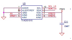
I am currently using a ADS1015 to catch the voltage from a thermistor  bridge circuit.

The configuration of ADS1015 is  0x4283. AINp=AIN0 AINn=GND, FS=+/-4.096V, continuous conversion mode, 1600SPS.

Input signal voltage range is 1.0V to 2.2V. VDD of ADS1015 is 3.3V.

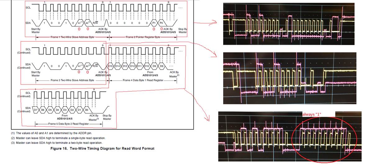
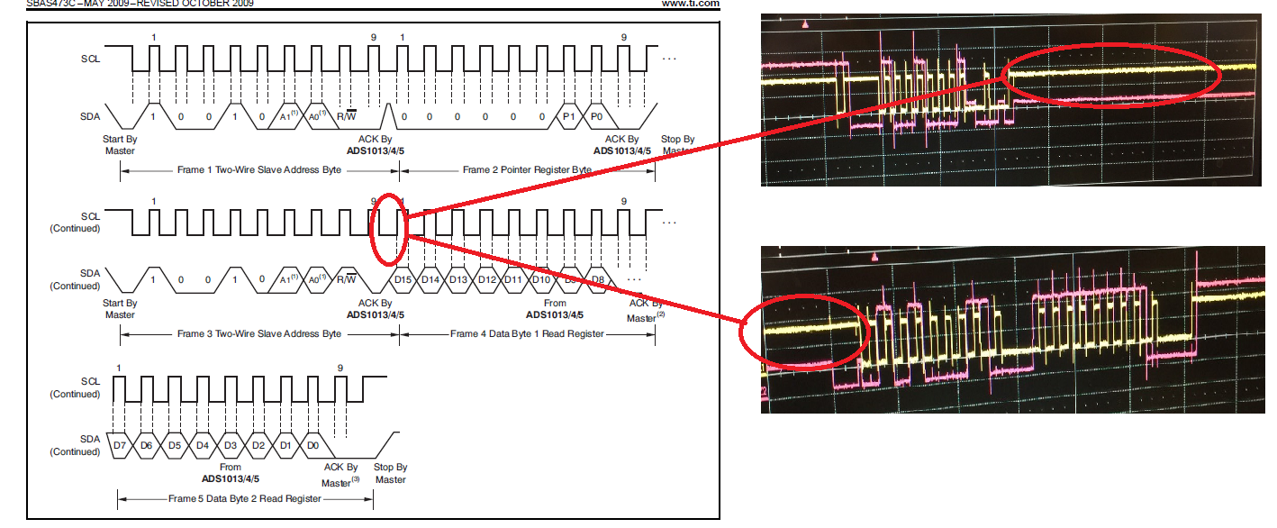
My issue is when I try to read the conversion result, I can get first byte of data correctly, but the second byte of data is always "1".

Please see the picture below. Thanks.

  • Hill,

    Thank you for your query. We will get back to you on this one shortly.

    Thanks,
    Krunal
  • Hill,


    I've looked over your I2C communications, and I don't see anything wrong with the way you have read the conversion. Byte 1 sends a write request to the device, the byte 2 writes 00 for the conversion register. Byte 3 sends the read request and bytes 4 and 5 should be the conversion data. It looks like the master or slave ack after each byte. However, it does look like the data is wrong since the output code shouldn't have written 1s in the last four bytes.

    Can you provide a schematic? It might help to verify the I2C address. Are there any other I2C address devices on this bus that might interfere with communications?

    Are you using the default configuration? What do you write to the configuration register? I would also try changing the second byte in the device read to 01h so that the device reads the configuration register, just to make sure the read and write work properly.


    Joseph Wu
  • Hi Joseph,

    Good day, thanks for your reply.

    Below picture is the schematic of ADS1015 in my design. There is no other device on this bus. There are 1k ohm pull-high resistor on SCL and SDA line, but it doesn't show on this picture.  

    The configuration of ADS1015 is  0x4283. AINp=AIN0 AINn=GND, FS=+/-4.096V, continuous conversion mode, 1600SPS. Input signal voltage range is 1.0V to 2.2V. VDD of ADS1015 is 3.3V.

  • Hill,

    Ok. Then as I mentioned in the last post, can you please read back the configuration register? Capture the SDA and SCL with the oscilloscope. Having the scope shots was very helpful.

    Joseph Wu

  • Hill,


    One other thing to keep in mind is that when power is applied to the device, it comes up without starting a conversion. When you first write to the device, make sure that a 1 is written into bit 15 of the config register. Later, read back the device and report what you read in the conversion register. It would also help to know what voltage you have on the input pins so that we can compare what the input voltage is vs the input range and see if it matches the output data.


    Joseph Wu
  • Hi Joseph,

    Thanks for your help. I've fixed this issue. The root cause is it should be keep "Low" between clock 9 and clock 1. Now I can get the data correctly. thanks.

  • Hill,


    I'm glad that you were able to find a solution. At first I thought it looked like a STOP condition but SDA doesn't return high. However, it almost looks like the SCL returning high may be interpreted as an extra SCL pulse, which shifts off the I2C communications.

    Regardless, if you have any other questions feel free to post back to the forum.


    Joseph Wu