This thread has been locked.

If you have a related question, please click the "Ask a related question" button in the top right corner. The newly created question will be automatically linked to this question.

ADS124S08: How to measure four 3-wire RTDs

Other Parts Discussed in Thread: ADS124S08, ADS1220, ADS124S06, ADS1118

Hi Joachim,

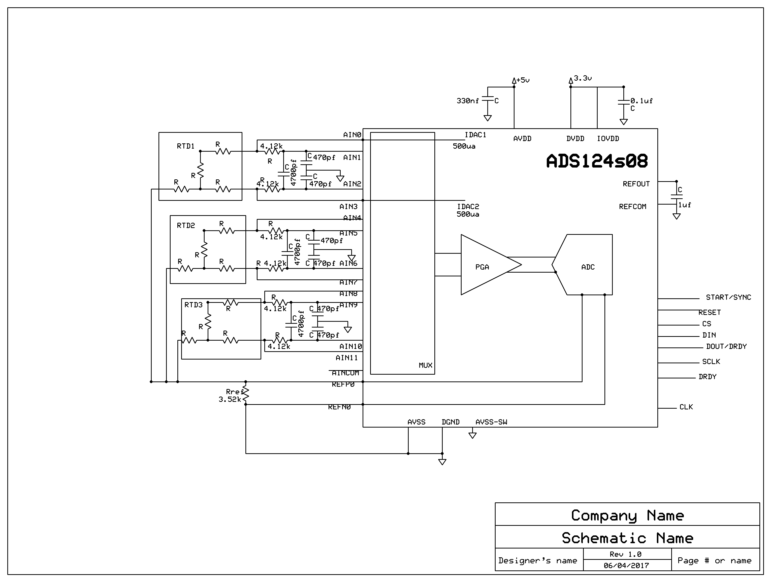
I need also to connect four 3-wires RTD to a MCU. There are many application notes to connect one 3-wire RTD but

I cannot find any schematic drawing about multiple RTDs connection.

You said "There are many ways how multiple RTD measurements can be implemented with one of our ADCs."

What is the best and more reliable and precise way ? Which ADC can suit exactly this need without additional circuitry

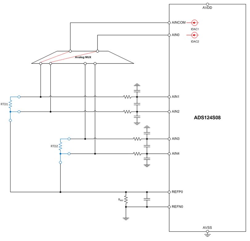
or additional software calculation (like 2 measurements and substraction as you explained with ADS124S08) ?

Which schematic and products do you recommend: 

1) ADC with only one RTD connected at a given time and  MUXs between ADC and MCU or

2) ADC allowing to directly connect four RTDs ?

3) a mix of these 2 solutions, for instance ADC with 2 RTDs and a MUX to switch 2/2 RTDs

Can you indicate pros and cons of these 2 extreme solutions ?

Thanks a lot in advance for your advice.

  • Salut Philippe,

    thank you for your question and welcome to our forum. I have split your post into a new thread to better track it.
    We are working on some collateral this year that will show how to measure multiple RTDs with our ADCs.

    It is hard for me to say which method will be the best, precise and most reliable implementation.
    I would think 2x ADS124S08 with two 3-wire RTDs connected to each ADS124S08 might probably the most precise option. But you could also measure every RTD individually with an ADS1220 for example.

    Joseph shows in the following post (e2e.ti.com/.../2097353) how to measure up to three 3-wire RTDs with one ADS124S08.
    In order to measure four you would need to use external MUXs which could potentially degrade the performance slightly.
    None of our ADCs can measure four 3-wire RTDs without the need for additional external circuitry.

    To find the most suitable solution for you, it would be good to know how quickly you need to measure all four RTDs, if you have space and/or cost constraints etc.

    The disadvantage of using four individual ADCs might be cost and PCB space. Also you would have to calibrate four ADCs and use four 'expensive' high precision reference resistors.
    The 'cheapest' solution might be to use one ADC with external MUXs. Disadvantage might be the settling time when switching between the RTDs. This might limit you on how fast you can measure all four RTDs.

    In terms of ADCs I would recommend either ADS124S08 or ADS1220.

    Regards,

  • Bonjour Joachim,

    Thank you for your very clear answer.

    My application is a temperature controller for ovens, the temperatures are changing very slowly, so the speed is not at all a concern; if I got

    4 temperature measurements (at different places in the oven's volume) every second it is enough ! 

    I have not any space constraint either.

    The only constraints are the precision and the cost.

    So I think the best choice for my application will be one ADS1220 and one 2:8 MUX.

    For the MUX, is the model CD4052 below suitable ?

    When you say "use external MUXs could potentially degrade the performance slightly", is it only a longer time to measure the four RTDs or

    do you speak also about precision of measurement ?

    Best regards, Philippe

  • Bonjour Philippe,

    thanks a lot for the additional information. Our ADCs are actually widely used in such kind of temperature controllers.

    The ADS124S08 or ADS124S06 (lower channel count version of ADS124S08) will in general offer better precision, accuracy and resolution than the ADS1220 as it is a higher performance device.

    My personal favorite solutions for the requirements you are describing would be:

    • Two ADS124S06 and two 3-wire RTDs per ADC or
    • One ADS124S08 with an external 2x 1:4 MUX to route the excitation currents to the different RTDs as shown below (I only show 2 RTDs but you can extend the concept to 4 RTDs as well). I believe something like an CD4052 that you are suggesting should work.

    With ADS1220 you would need one 2x 1:4 MUX to route the voltages across the RTDs to one analog input pair of the ADC and then another 2x 1:4 MUX to route the two excitation currents to the RTDs. This solution should work as well. But as mentioned before, if you are looking for best performance then the ADS124S0x solutions would be preferred.

    Depending on the circuit implementation and where in the signal chain the MUXs are placed, either the channel-to-channel leakage current, the channel-to-channel resistance matching or the channel on-resistance of the MUX can influence the measurement accuracy.

    Regards,

  • Dear Joachim,

    Thanks a lot for your quick answer.

    I understand the solution number 1 with 2 x ADS124S06 and the solution number 2 with one ADS124S08 plus one external 2x 1:4 MUX. (sorry I called this MUX "2:8" and it is rather "2x1:4" !)

    1) But can you explain why you need two 2x1:4 MUXs in the solution 3 with one ADS1220.
    In my understanding one 2x1:4 MUX is enough, because one wire of each RTD is permanently connected to RREF/RF3/REPFP0 and the 2x1:4 MUX will connect alternatively the 2 other wires of each RTD to RF1/AIN1 and RF2/AIN0. (I am referring at figure 77 of ADS1220 datasheet www.ti.com/.../ads1220.pdf)

    2) At this stage I can also consider the alternative to use four J-thermocouples instead of four 3-wires RTD (temperatures to measure are in the 0-300°C range). What do you recommend as ADC model and schematic drawing in this hypothesis ?

    Best regards, Philippe
  • Hi Philippe,

    let me know if the following clarifies things:

    1) The schematic drawing above might be a little misleading, because I do not show the lead resistances of the RTDs.
    Following is a new drawing showing a potential solution with ADS1220 (again only for 2 RTDs, but you can extend the concept to 4 RTDs as well of course).
    In order to implement the lead resistance compensation using the two excitation current sources you will need one 2x 1:4 MUX to route the excitation currents to the RTDs. The 2nd 2x 1:4 MUX is needed to route the RTD voltage to the ADC inputs.


    2) The ADS124S08 would be the best and most accurate single device solution to measure 4 thermocouples, but an ADS1220 with an external MUX would work as well.
    The connection of each thermocouple to the ADC would e.g. be implemented as shown in the ADS1220 datasheet.
    You need some means to bias the thermocouple to within the voltage range of the ADC. This can be implemented in multiple ways. What we usually show is the implementation using a pullup and pulldown resistor to the supplies (In case you have grounded thermocouples we need to implement this slightly differently). Besides biasing the thermocouple, this implementation can also serve to detect a broken thermocouple wire. Following the pullup/down resistors you would put a RC filter.
    You will also have to measure the cold junction temperature then. Customers use all different types of temperature sensors to measure the cold junction temperature: diodes, thermistors, RTDs, analog/digital output temperature sensors, etc.

    Regards,

  • Hi Joachim,

    I am sorry but I continue to not understand why you need 2 MUXs. I miss something for sure, I will try to make a drawing tomorrow.

    About the thermocouple solution, what is the maximum number of thermocouples I can connect to an ADS124S08 ?

    Philippe
  • Hi Philippe,

    my apologies. I am waiting for your drawing then. Maybe you even have a smarter solution to implement the measurement. I am always interested in learning news ways.

    You could measure up to 6 thermocouples with one ADS124S08 without having to use an external MUX.
    And in case you could connect all thermocouples together on one side, you could even measure up to 12.
    However the maximum numbers of thermocouples you can measure also depends on the method you want to choose for measuring the cold junction temperature.

    Regards,
  • Hi Joachim,

    it is probably a bad idea to do this wiring with only one MUX (sorry for the bad drawing):

    Philippe

  • Hi Joachim,

    About the maximum number of thermocouples, 6 or 12, that can be measured with a ADS124S08, I think that it depends on the

    thermocouple junction type, insulated, grounded or exposed :

    As I am not sure of using always the same type of thermocouple junction, I think that connecting only 6 thermocouples, each thermocouple

    using 2 inputs of ADS124S08  is the best choice. Do you agree ?

    To know the reference junction temperature, can I use the internal temperature sensor of the ADS124S08 ?

    Philippe

  • Hi Philippe,

    the circuit you have drawn above using ADS1220 will work in general.
    The only drawback of routing the excitation currents through the same MUX that is used for the measurement is, that the Ron - especially the Ron matching of the MUX channels - and leakage currents will have an impact on the measurement accuracy.
    For example in CD4052 the Ron between channels changes by a couple of Ohms. The current sources will then generate different voltage drops across the MUX channel Rons. This in turn will lead to a differential offset error in your reading and thus introduce a big temperature reading error.
    You could in principle also route the excitation currents sources to AIN0, AIN1 in above drawing. But then the excitation currents would have to flow through the series filter resistors. You would then have to choose precisely matched resistors and could not make them too large also. Many customers use filter resistors in the 1k to 10kOhm range because they also use the resistors to limit the current into the ADC pins (<10mA) in an overvoltage event.
    In short, yes this solution will work, but if you are looking for best accuracy then I would not recommend it.

    Yes, I would agree with you on the thermocouple configuration. Limit it to 6 thermocouples with ADS124S08 and use one dedicated differential input pair for each thermocouple.
    However you need to be careful with grounded thermocouples depending on how the thermocouple GND and your system GND are connected. In many cases this will call for a bipolar analog supply for the ADC.

    I don't recommend to use the ADS124S08 internal temperature sensor for the cold junction temperature measurement mainly because of two reasons:
    1) The accuracy of the internal temperature sensor is not good enough (around 1°C to 3°C without calibration). You could potentially run over-temperature calibration of it but that might be costly in your end production.
    2) Often times you cannot place the device close enough to the cold junction to measure the true junction temperature.

    When using multiple thermocouples, you sometimes even need to measure the junction temperature at multiple points in case you can have a temperature gradient across your junction. But this all depends on what your accuracy requirements are.

    Regards,
  • Hi Joachim,

    Thanks a lot for your very clear answer about the use of 2 MUXs in front of ADS1220. I will follow your recommendation.

    About number of thermocouples that can be attached to an ADS124S08, the maximum number of 6 but this number will be reduced to 4 if I connect a RTD to measure precisely the cold junction temperature. I am wondering now if some electrical terminal are supplied with a RTD already inside or are intended to install a RTD inside ?

    Best regards, Philippe

  • Hi Philippe,

    you are correct. If you want to measure the cold junction temperature with ADS124S08 as well, then the maximum number of thermocouples you can measure (without using an external MUX) will reduce.

    In case you would use an analog output temperature sensor, you would only need two analog inputs of the ADS124S08 (one to connect to GND and one to connect to the temp sensor output).
    In case you want to use an RTD - in most cases a 2-wire RTD is sufficient - you would need three analog inputs (one for the excitation current output, two for the RTD measurement) and the REFP0, REFN0 inputs.
    So in both cases you could still measure up to 5 thermocouples.

    I am sorry, but I didn't understand the question in your last sentence.

    If you want to develop one single board that can be used for both thermocouple and 3-wire RTD measurements we can probably make that work. You can either accomplish this by not populating certain components on the board or by using switches to switch in an out certain resistors.

    Regards,
  • Hi Joachim,

    Yes you are right, a 2-wire RTD should be enough to measure junction temperature.

    My question was about the practical aspect to insert a RTD inside the junction ? Do some junction terminals and some RTD exist to do that easily ?

    For now, thanks to your advices, my design could be:

    - a main board with one ADS124S08 and three 3-wires RTD, that is enough for most of our applications (2 RTD for oven temperature regulation

    and 1 RTD for security)

    - one additional board with one ADS124S08, 5 thermocouples and 1 RTD (cold junction) that can be added as an option

    in case we need to measure temperature of the products that are treated in the oven, that is not the general case, it just can happen sometimes.

    I will use SPI data transfer between the main board and the additionnal board. The distance between the 2 boards should not exceed  50 cm, do you

    think this design is correct ?

    Thanks a lot, Philippe

  • Hi Philippe,

    I am unfortunately not an expert when it comes to mechanics and how to best connect the RTD to the cold junction. This depends a lot on how you design your cold junction/thermal block.
    The following reference design (www.ti.com/.../tipd109) talks a little bit about how a temperature sensor can be 'embedded' into the thermocouple connector. In this reference design the internal temperature sensor of ADS1118 is used. The ADS1118 integrates a higher precision temperature sensor than ADS124S08.
    However with multiple thermocouples you need to come up with a different solution to make sure the cold junction temperature of all thermocouple connectors is the same.

    I don't see anything wrong with your design approach. Once you have a schematic we will be happy to review it. We can do that offline by email then if you prefer.

    Regards,
  • Hi Mr Joachim,

    I am a intern student who work for Mr philippe and this is my schematic for one ads124s08 connect with 3 pt100. 

    I have a question about the RC filter between pt100 and ads124s08, in my opinion, the pt 100 will give a volts d.c. so we need to set a cut-off frequency as low as possible. It is possible to ues these valeur for capacitance and resistance?

    Look forward to your favourable reply,

    Regards,

    Haoliang QIN

  • Hi Haoliang,

    thanks a lot for sharing your schematic with me. There are a few things I would like to point out before commenting on the RC filter selection.

    The voltage generated across Rref will set the common-mode voltage for the RTD and thus the PGA. I usually recommend to set the voltage across Rref somewhere close to AVDD/2 or below. With the settings you are showing you would probably use a PGA gain of 8 or 16, depending on how high temperatures you want to measure with the RTD. If you need to measure temperatures up to 850°C you need to limit your PGA gain to 8 in your setup.
    I would recommend reducing Rref to a value somewhere between 2k and 2.5kOhm.
    What is the maximum RTD temperature you need to measure?

    You should place a differential cap across the REFP0/REFN0 inputs in parallel to Rref.

    Do you anticipate any overvoltages that can occur on the RTD terminals?
    If so then we need to make sure we sufficiently protect all inputs which are connected to those terminals. The first line of defense for protecting the inputs is to limit the current into the device to <10mA in case of an overvoltage event. This can be accomplished by placing series resistors on each input. Additional protection (TVS diodes, Schottky diodes, ferrites, etc) might be required depending on your requirements.

    Following are some of my general guidelines for selecting the RC filter values:

    • Select the smallest possible R value that will limit your input current to 10mA at the maximum expected overvoltage. You want some margin of course.
      If you want to protect for voltages up to 40V, you would for example use a 4.7kOhm or larger series resistor.
    • Select a differential cap value to get a corner frequency a decade (or more) below the modulator frequency (fMOD=256kHz for ADS124S08) so that you get at least 20dB attenuation at the modulator frequency from the RC filter. Setting the corner frequency at the output data rate or 10x above is usually a good starting point.
    • In case you want to place common-mode caps as well, make them at least 10x smaller than the differential cap. You have done that correctly already.

    I would not recommend making the corner frequency too small. The reason is, that when changing from one RTD measurement to the next one, the settling time of the analog signal might become too large.

    Regards,

  • Hi,Joachim Wurker

    I just need to measure temperatures up to 300°C. We have a Current source (IDAC=500ua), in this situation, rt100=212.02ohm, so overvoltage is 0.106V?

    What's more how can i find out the value to the cap which is  parallel to Rref?

    Regards,

    Haoliang QIN

  • Hi Haoliang,

    I am sorry for not being clear with my statement about 'overvoltages'. What I meant by that is if the terminals where the RTD is being connected to can see any high voltages due to for example incorrect wiring. Your end-customer might for example accidentally short one of the terminals to a 24V line or something like this.
    In case the RTD is located on your PCB and not exposed to the environment outside your module, then you probably do not need a lot of protection.

    Regarding the differential capacitor value selection, you might want to study the following application note:

    Regards,

  • Hi Mr Joachim,

    Thanks to you domcument supply, i draw a new schematic for my equipment.

    In this version, i change the Rref and i reset my RC filter. In this case, Differential-Mode Corner Frequency is 361hz and 

    Common-Mode Corner Frequency is 7726hz. When Rref=2Kohm, we have (2*500ua)*2Kohm=2v,2v<2.5(below than AVDD/2).

    And i also use a RC filter for REFP0 and REFN0 to have a better precision.

    But i am still confuse to corner frequency, both of them is above 50hz, it is possible to interference by Alternating Current/voltage? What's more if i want to have the best preformance in precision, can i set the corner frequency much lower than 50hz? (Because i think in our product(oven) , the temperature can't changer very quickly, so compare to precision, time of changing form one pt100 to another is not very important. )  

    Look forward to your favourable reply,

    Regards,

    Haoliang QIN

  • Hi Haoliang,

    thanks a lot for sharing this update.

    With an Rref =2kOhm your system should work fine for RTD temperatures up to 300°C. You could use a PGA gain = 16 in that case.

    If you are not worried about overvoltages then I would suggest reducing the series resistor values further. Use 1kOhm or 470Ohm for example and increase the filter capacitor values accordingly.
    I would also suggest to put series resistors on all inputs where your internal current sources are routed to. That will protect those inputs a little as well then.

    I personally don't think a full filter is necessary on the reference inputs. But you should provide provisions for it for your first prototype so you have the option to play around with it.
    You will probably be fine with only a series resistor on REFP0 and the differential capacitor.

    In order to reject 50Hz and 60Hz noise I recommend to use one of the data rates of the ADS124S08 which offer 50Hz and/or 60Hz rejection.
    If you are not worried about settling times in your system then you could certainly also reduce your filter corner frequencies to below 50Hz. But I don't think this is very practical because all your filter values are getting quite big then.

    Regards,
  •  Mr Joachim,

    following your advise, I make some change to my schematic.

    After reading the datasheet of ADS124s08, i have question about the digital filter, in page 43, there is a table explain how we make a 50Hz and/or 60Hz rejection.

    Do we need to declare something in our microprocessor (STM32f407vg)? I mean do we need to progammer our ads for this filter or il wiil automatically set by ADS124s08?

    Regards,

    Haoliang QIN

  • Hi Haoliang,

    I see that you set your filter corner frequency at around 25Hz now. This will not help you very much in rejecting 50Hz noise. You would have to set the corner frequency at 5Hz to at least get 20dB rejection of 50Hz noise. But as you can see your capacitor values get really large then.
    If you can use one of the data rates <=50SPS then I would really recommend to rely on the rejection of the digital filter and use a higher filter corner frequency.

    All you need to do to get 50Hz and/or 60Hz rejection from the digital filter inside the ADS124S08 is to program the data rate in the DATARATE register (bits DR[3:0]) to one of the data rates mentioned in Tables 16 and/or 17.
    You can also select between the low-latency and the SINC3 filter using the FILTER bit.

    Regards,

  •  Mr Joachim,

    So i still use my second schematic but just change those resistor (1Kohm) and mycorner Frequency is probably 3.1Khz ( a decade ( below the modulator frequency,fMOD=256kHz ), and then to to get 50Hz and/or 60Hz rejection from the digital filter, i need to program the data rate in the DATARATE register.Am i correct?

    I thing i don't quite understand about the data rate, the data rate here is mean rate of read (ads124s08 mesure the value of pt100) or rate of output (ads124s08 envoyer information to STM32) ?

    Look forward to your favourable reply,

    Regards,

    Haoliang QIN

  • Hi Haoliang,

    yes, your filter values look fine. In your case the corner frequency of the differential filter is actually 1.56kHz, because you need to include the 1kOhm resistor two times in the formula. There is no real wrong or right about the filter values. You may have to play around with them during evaluation.
    You now need to select a data rate and the filter type that gives you the desired rejection at 50Hz and 60Hz. A good starting point is usually to use '20SPS and the low-latency filter' or '10SPS and the SINC3 filter'.

    I didn't really understand your 2nd question. The data rate refers to the output data rate of the ADS124S08. That means how often a new conversion result is available from the ADC.

    Regards,
  • Mr Joachim,

    According to your advice, i draw this schematic

    But when i config this ads124s8, the temperature of this ADC  is very hot, is it normal?

    Regards,

    Haoliang QIN

  • Hi Haoliang,

    your schematic looks correct as far as I can see. The power dissipation should only be around 5-10mW in your case. Therefore the device should not really be getting hot.

    Are you able to communicate with the ADS124S08?
    What are your register settings?
    Could you double check that you did not accidentally miswire any pins?

    Regards,
  • Hi Joachim,

    I am able to send my command to set up my ads but there is no feedback, like this photo:

    0x07 is the command reset, then 0x42,0x00,0x12 is command Command Mux register Ain1:0001 Ain2:0010 ,ect, 

    My register settings : -device id register(add=00h) : is read only so i do nothing to this register.

           -device status register(01h) : also read only.

           -Mux register(02h) : ain1 and ain2 :0x12.

           -gain setting register(03h) : 14.Tmod, PGA enabled, gain select 16;0x0c.

           -Data rate register(04h) : Global chop enble : disabled, internal oscillator,signle-shot,low-latency filter,2.5SPS: 0x30.

           -reference control(05h) : disabled reference monitor,disabled the positive reference buffer,disabled the negative reference buffer, internal 2.5v

                                      reference, internal reference is always on, even in power-down mode.  0x3a.

           -excitation current register1(06h):500uA:0x05

           - excitation current register2(07h) idac2:AIN3,idac1 AIN0 :0x30

          - sensor blasing register(08h) : 0x00.

          -System Control(09h) :

    And i didn't config the calibration register yet.

    I think it is possible that i  miswire some pins, because i use a adaptor (IC51-0324-805,tqfp32 to dip32) to do the wiring.like this one

    the distance between 2 pin is so close so maybe it will miswire some pins when i close it.

    Regards,

    Haoliang QIN


  • Hi Haoliang,

    I want to make a few general comments first:

    • Make sure to use the correct SPI mode.
      The interface operates in SPI mode 1 where CPOL = 0 and CPHA = 1. In SPI mode 1, SCLK idles low and data are launched or changed only on
      SCLK rising edges; data are latched or read by the master and slave on SCLK falling edges.
      It seems like your SCLK does idle high.
    • Make sure to wait at least 4096 · tCLK after sending the RESET command to allow the reset process to complete.
      Sending the RESET command is optional because the device already performs a power-on reset when power is applied.
    • In order to debug your SPI communication I suggest you try to read a register first. Once that is working properly you can worry about writing registers.
    • In order to check if the device is operating at all you could simply take the START pin from low to high using the default register settings.
      You should then see the /DRDY signal fall after approx. 57ms.

    Regarding your register settings:

    • You should enable the positive reference buffer.
    • You need to enable the internal 2.5V VREF, but select the external REFP0/REFN0 inputs for the ADC.

    Regards,

  • Mr Joachim,

     Follow your advices , I check my programme but i cant' find out the problem. According to the Oscilloscope all the command send by stm32 is correct but my ads124s08 always no reply.

    In this projet i will just use one ads so can i connect CS to Ground directly? 

    I will send you my code which is coder en Keil4, would you please help me to find out the problem?

    Regards,

    Haoliang QIN

    main.h

    ADS124S08.h

    GET_Temp.c
    /*
    *Driver for ADS124S08 created by Haoliang QIN at 20/04/2017
    *COPYRIGHT 2017 France Etuves
    *Version V1.0
    */
    
    #include "GET_Temp.h"
    
    vu16 GetTemp(u32 advalue)
    {
         vu32 Vtemp_sensor;			
         vu16 Current_Temp;
    		 vu8 R;
         
    
         Vtemp_sensor = (((vu32)advalue )/16777215)*5;  
         R= Vtemp_sensor/0.0005; //500Ua
    	   Current_Temp=(R)/0.385;
         return Current_Temp;
    }  
    

    ADS124S08.c
    /*
    *Driver for ADS124S08 created by Haoliang QIN at 20/04/2017
    *COPYRIGHT 2017 France Etuves
    *Version V1.0
    */
    
    #include "ADS124S08.h"
    
    u8 FFF;
    SPI_InitTypeDef SPI_InitStructure;
    GPIO_InitTypeDef GPIO_InitStructure;
    
    void Delay_ms(u16 time){
    	u16 i = 0;
    	while(time--){
    		i = 12000;
    		while(i--);
    	}
    }
    
    
    void GPIO_ExternalADC_Cfg(void)
    {
    
    
        RCC_AHB1PeriphClockCmd(RCC_AHB1Periph_GPIOA, ENABLE);
    	  RCC_AHB1PeriphClockCmd(RCC_AHB1Periph_GPIOB, ENABLE);
    	  RCC_AHB1PeriphClockCmd(RCC_AHB1Periph_GPIOC, ENABLE);
    	
    	
        /* <-- Configures Exteranl_ADC pins: START(PB.2) and RESET(PB.0)  --> */
        GPIO_InitStructure.GPIO_Pin =  GPIO_Pin_0;
    	  GPIO_InitStructure.GPIO_Pin =  GPIO_Pin_2;
        GPIO_InitStructure.GPIO_Mode = GPIO_Mode_OUT;
    		GPIO_InitStructure.GPIO_OType=GPIO_OType_PP;
        GPIO_InitStructure.GPIO_Speed = GPIO_Speed_50MHz;
        GPIO_Init(GPIOB, &GPIO_InitStructure);
        //ExternalADC_START_LOW;
    		GPIO_ResetBits(GPIOB, GPIO_Pin_2);
       //ExternalADC_/R/E/S/E/T_HIGH();
    		GPIO_ResetBits(GPIOB, GPIO_Pin_0);
    		GPIO_SetBits(GPIOB, GPIO_Pin_2);
    	  GPIO_SetBits(GPIOB, GPIO_Pin_0);


    	/* <-- Configures Exteranl_ADC pins: Flags(PB.3) --> */
        GPIO_InitStructure.GPIO_Pin = GPIO_Pin_3;//
        GPIO_InitStructure.GPIO_Mode = GPIO_Mode_IN;//
        GPIO_InitStructure.GPIO_Speed = GPIO_Speed_50MHz;
    		GPIO_InitStructure.GPIO_PuPd = GPIO_PuPd_NOPULL;
        GPIO_Init(GPIOB,&GPIO_InitStructure);
        /* <-- Configures Exteranl_ADC_SPI start --> */
        /*!< Configure Exteranl_ADC_SPI pins: SCK, MOSI, MISO CS*/
        GPIO_InitStructure.GPIO_Pin = GPIO_Pin_10|GPIO_Pin_12; //SCK,NSS(CS)
        GPIO_InitStructure.GPIO_Speed = GPIO_Speed_50MHz;
        GPIO_InitStructure.GPIO_Mode = GPIO_Mode_AF;
    		GPIO_InitStructure.GPIO_OType=GPIO_OType_PP;
    		GPIO_InitStructure.GPIO_PuPd = GPIO_PuPd_NOPULL;
        GPIO_Init(GPIOB, &GPIO_InitStructure);
    		
    		GPIO_InitStructure.GPIO_Pin = GPIO_Pin_2|GPIO_Pin_3; //MISO,MOSI
        GPIO_InitStructure.GPIO_Speed = GPIO_Speed_50MHz;
        GPIO_InitStructure.GPIO_Mode = GPIO_Mode_AF;
    		GPIO_InitStructure.GPIO_OType=GPIO_OType_PP;
    		GPIO_InitStructure.GPIO_PuPd = GPIO_PuPd_NOPULL;
        GPIO_Init(GPIOC, &GPIO_InitStructure);
    				
    		GPIO_PinAFConfig(GPIOB, GPIO_PinSource10, GPIO_AF_SPI2);//SCK
    		GPIO_PinAFConfig(GPIOB, GPIO_PinSource12, GPIO_AF_SPI2);//NSS
    		GPIO_PinAFConfig(GPIOC, GPIO_PinSource2, GPIO_AF_SPI2);//MISO
    		GPIO_PinAFConfig(GPIOC, GPIO_PinSource3, GPIO_AF_SPI2);//MOSI
       
        /* <-- Configures Exteranl_ADC_SPI end --> */		
    }
    /**
      * @brief  Configures SPI2 for External ADC interface.
      *     Master mode,8b,f=31250KHz
      * @param  None
      * @retval None
      */
    void Init_ADC_SPI(void)
    {
    // 		RCC_APB1PeriphResetCmd(RCC_APB1Periph_SPI2, ENABLE);
    // 		RCC_APB1PeriphResetCmd(RCC_APB1Periph_SPI2, DISABLE);
    		RCC_APB1PeriphClockCmd(RCC_APB1Periph_SPI2, ENABLE);
        SPI_InitStructure.SPI_Direction = SPI_Direction_2Lines_FullDuplex;
        SPI_InitStructure.SPI_Mode = SPI_Mode_Master;
        SPI_InitStructure.SPI_DataSize = SPI_DataSize_8b;
        SPI_InitStructure.SPI_CPOL = SPI_CPOL_Low;//CPOL=0
        SPI_InitStructure.SPI_CPHA = SPI_CPHA_2Edge;//CPHA=1
        SPI_InitStructure.SPI_NSS = SPI_NSS_Soft;
        SPI_InitStructure.SPI_BaudRatePrescaler = SPI_BaudRatePrescaler_128;//Fsck=PCLK1/256=31250Hz,PCK1=8000000hz
        SPI_InitStructure.SPI_FirstBit = SPI_FirstBit_MSB;
    	//SPI_InitStructure.SPI_CRCPolynomial = 7;
        SPI_Init(SPI2, &SPI_InitStructure);
        /* Disable SPI2 CRC calculation */
        //SPI_CalculateCRC(SPI2, DISABLE);
        /* Enable SPI2 */
        SPI_Cmd(SPI2, ENABLE);
    		
    // 		SPI_SendByte(0x00);
    // 		Delay_ms(500);
    }
    
    void SPI2_ConfigADS_par_STM32(void)
    {
    
    		SPI_SendByte(0x06); //Command RESET
    	
    	  Delay_ms(500);
    	
    		SPI_WriteAReg(Reg_INPMUX, 0x12);//Command Mux register Ain1:0001 Ain2:0010 A tester
    		SPI_WriteAReg(Reg_PGA, 0x0c);//Command Gain setting 14.Tmod:000 PGA enabled:01 PGA_select_16:100  � tester
    		SPI_WriteAReg(Reg_DATARATE, 0x30);//Command Data_Rate G_chop_disabled:0 CLK_internal:0 Mode_single_shot:1 latency;1 Data_rate selection_2.5SPS: 0000?tester	
    		SPI_WriteAReg(Reg_REF, 0x12);//Command reference control  tout par default sauf REFCON,internal 2.5v ref ?tester	  
    		SPI_WriteAReg(Reg_IDACMAG, 0x05);//Command Excitation current page75 ,500uA , ?tester	  	 
    		SPI_WriteAReg(Reg_IDACMUX, 0x30);//Command Excitation current page76 ,idac2:AIN3,idac1 AIN0 , ?tester	  		 
    		SPI_WriteAReg(Reg_VBIAS, 0x00);//Command sensor blasing page77 , , � tester	  		 
    		SPI_WriteAReg(Reg_SYS, 0x10);//Command System Control tout par default , �  tester	 
    
    }
    
    void SPI_SendByte(u8 data)
    {
    	while (SPI_I2S_GetFlagStatus(SPI2, SPI_I2S_FLAG_TXE) == RESET);
    	SPI_I2S_SendData(SPI2, data); 
    	while (SPI_I2S_GetFlagStatus(SPI2, SPI_I2S_FLAG_RXNE) == RESET); 
    	SPI_I2S_ReceiveData(SPI2); 
    }
    
    u8 SPI_ReadByte(u8 data)
    { 
    	while (SPI_I2S_GetFlagStatus(SPI2, SPI_I2S_FLAG_TXE) == RESET);
    	SPI_I2S_SendData(SPI2, data); 
    	while (SPI_I2S_GetFlagStatus(SPI2, SPI_I2S_FLAG_RXNE) == RESET); 
    	return SPI_I2S_ReceiveData(SPI2); 
    }
    
    void SPI_WriteAReg(u8 add, u8 data)
    {
    	SPI_SendByte(0x40 + add);
    	SPI_SendByte(0);//Num de Reg:1
    	SPI_SendByte(data);
    }
    
    
    u8 SPI_ReadAReg(u8 add)
    {
    	SPI_SendByte(0x20 + add);
    	SPI_SendByte(0);
    	return SPI_ReadByte(0);
    }
    
     u32 SPI_RDATA(void)
    {
    	u32 Data;
    	SPI_SendByte(0x12);//RDATA
    	Data = SPI_ReadByte(0);
    	Data <<= 8;
    	Data += SPI_ReadByte(0);
    	Data <<= 8;
    	Data += SPI_ReadByte(0);	
      return Data;
    }


    /************************ (C) COPYRIGHT France Etuves *****END OF FILE****/
    

    1321.main.c
    //Projet created by YAN 6/04/2017 19:45
    #include "stm32f4xx.h"
    #include "ADS124S08.h"
    #include "GET_Temp.h"
    
    u8 f1;
    u8 f2;
    u8 f3;
    u32 ft;
    u16 T;
    
    // void Delay_ms(u16 time){
    // 	u16 i = 0;
    // 	while(time--){
    // 		i = 12000;
    // 		while(i--);
    // 	}
    // }
    
    int main(void){
    	Delay_ms(800);
    	Init_ADC_SPI();
    	GPIO_ExternalADC_Cfg();
    	SPI2_ConfigADS_par_STM32();
    	
    	f1=SPI_ReadAReg(Reg_ID);
    	f2=SPI_ReadAReg(Reg_STATUS);
    	f3=SPI_ReadAReg(Reg_INPMUX);
    while(1){	
    	
    	Delay_ms(800);
    	SPI_SendByte(0x00);
    	SPI_SendByte(0x00);
    	SPI_SendByte(0x08);//start
    	Delay_ms(800);
     	ft=SPI_RDATA();
    	SPI_SendByte(0x0A);//stop
    	T=GetTemp(ft);
    	Delay_ms(500);
    }
    
    }
    

    GET_Temp.h

  • Hi Haoliang,

    I am sorry to hear that you are still struggling to communicate with the ADS124S08.
    According to your earlier scope picture the ADS124S08 seems to respond somehow on DOUT/DRDY. Therefore I would guess there is still something incorrect in your SPI setup.

    Did you already try any of my suggestions above?
    Did you make sure that SCLK idles low?

    If you only operate one ADS124S08 on the SPI bus you can tie /CS to GND.
    We generally recommend to use /CS even if only one device is on the bus, as long as you don't have any pin limitations on the MCU.
    /CS is useful to recover the SPI communication in case there are disturbances on the bus.

    Regards,
  • Hi Mr Joachim,

    I am very sure that SCLK idles low (CPOL=0, CPHA=1), for each command,

    void Init_ADC_SPI(void)
    {
    		RCC_APB1PeriphResetCmd(RCC_APB1Periph_SPI2, ENABLE);
    		RCC_APB1PeriphResetCmd(RCC_APB1Periph_SPI2, DISABLE);
    		RCC_APB1PeriphClockCmd(RCC_APB1Periph_SPI2, ENABLE);
        SPI_InitStructure.SPI_Direction = SPI_Direction_2Lines_FullDuplex;
        SPI_InitStructure.SPI_Mode = SPI_Mode_Master;
        SPI_InitStructure.SPI_DataSize = SPI_DataSize_8b;
        SPI_InitStructure.SPI_CPOL = SPI_CPOL_Low;//CPOL=0
        SPI_InitStructure.SPI_CPHA = SPI_CPHA_2Edge;//CPHA=1
        SPI_InitStructure.SPI_NSS = SPI_NSS_Soft;
        SPI_InitStructure.SPI_BaudRatePrescaler = SPI_BaudRatePrescaler_256;//Fsck=PCLK1/256=31250Hz,PCK1=8000000hz
        SPI_InitStructure.SPI_FirstBit = SPI_FirstBit_MSB;
    	//SPI_InitStructure.SPI_CRCPolynomial = 7;
        SPI_Init(SPI2, &SPI_InitStructure);
        /* Disable SPI2 CRC calculation */
        //SPI_CalculateCRC(SPI2, DISABLE);
        /* Enable SPI2 */
        SPI_Cmd(SPI2, ENABLE);
    		
    // 		SPI_SendByte(0x00);
    // 		Delay_ms(500);
    }

    i set a delay about 0.5s after the command reset

    void SPI2_ConfigADS_par_STM32(void)
    {
    
    		SPI_SendByte(0x06); //Command RESET
    	
    	  Delay_ms(1500);
    	
    	  SPI_SendByte(0x42);//WREG
    	  SPI_SendByte(0x7);//8reg
    		SPI_SendByte(0x12);
    		SPI_SendByte(0x0c);
    		SPI_SendByte(0x30);
    		SPI_SendByte(0x12);
    		SPI_SendByte(0x05);
    		SPI_SendByte(0x30);
    		SPI_SendByte(0x00);
    		SPI_SendByte(0x10);
    
    }

    And when i read Register i ues the code like this:

    SPI_SendByte(0x21);//RREG
    SPI_SendByte(0x07);//8Reg		
    	f1=SPI_ReadByte(0x00);
    	f2=SPI_ReadByte(0x00);
    	f3=SPI_ReadByte(0x00);
    	f4=SPI_ReadByte(0x00);
    	f5=SPI_ReadByte(0x00);
    	f6=SPI_ReadByte(0x00);
    	f7=SPI_ReadByte(0x00);
    	f8=SPI_ReadByte(0x00);

    But no metter how change my oscilloscope, there is always no respond.

    PS: I find than when i tie /CS to GND, f1~~f8 is 0x00. But when i tie /CS to a pin NSS ,f1~~f8 is 0xff. 

    Regards,

    QIN Haoiang

  • Hi QIN Haoiang,

    in one of your previous posts you showed an oscilloscope diagram where the device seemed to communicated somehow (it showed MISO and MOSI toggling). Is this not the case now anymore?

    The fact that you always read 0x00 when /CS is low, would tell me that the ADS124S08 might not receive the SCLK signal correctly.
    When /CS is high, DOUT/DRDY is Hi-Z. So in case you have a pull-up on that line somewhere then you would always read 0xFF. That is expected behavior.

    Did you try taking the START pin high after the device comes out of reset?
    You should then see /DRDY falling low after approx. 57ms. That would at least tell us that the ADS124S08 is working.

    Is the ADS124S08 still getting very hot?
    It seems like the positive reference buffer is still not enabled.

    Regards,
  • Mr Joachim,

    After that time, i can't find that signal anymore.

    Here is the code i ues to config start and reset:

     /* <-- Configures Exteranl_ADC pins: START(PB.2) and RESET(PB.0)  --> */
        GPIO_InitStructure.GPIO_Pin =  GPIO_Pin_0;
    	  GPIO_InitStructure.GPIO_Pin =  GPIO_Pin_2;
        GPIO_InitStructure.GPIO_Mode = GPIO_Mode_OUT;
    		GPIO_InitStructure.GPIO_OType=GPIO_OType_PP;
        GPIO_InitStructure.GPIO_Speed = GPIO_Speed_2MHz;
        GPIO_Init(GPIOB, &GPIO_InitStructure);
        //ExternalADC_START_LOW;
    		GPIO_ResetBits(GPIOB, GPIO_Pin_2);
       //ExternalADC_/R/E/S/E/T_HIGH();
    		GPIO_ResetBits(GPIOB, GPIO_Pin_0);
    		
    	  GPIO_SetBits(GPIOB, GPIO_Pin_2);
    	  GPIO_SetBits(GPIOB, GPIO_Pin_0);

    As it show, first i set start and /reset in low so that i can reset my ads, and then i set start and reset in high, am i correct?

    The ads is not very hot now.

    I check the datasheet, , in the  Reference Control Register (address = 05h), i set 0x12(00010010). According to datasheet, bit5(sixth bit)=0 mean enable the positive reference buffer.

    In fact i don' understand how to set this register, i tell me i need to enable the internal 2.5V VREF, but select the external REFP0/REFN0 inputs for the ADC,

    to use internal 2.5 Vref, i need to set bit3:2 to 10, to  select the external REFP0/REFN0 inputs, i need to set bit3:2 to 00. How can i do this in the same register?

    Regards,

    Haoliang QIN


  • Hi Haoliang QIN,

    after taking /RESET high, you need to wait the reset period before taking the START pin high. So I suggest you add another delay before taking START high.
    For now I would not communicate with the device at all after you took the START pin high, means leave the ADS124S08 in its default settings. Just check if you see the /DRDY signal fall low after 57ms. This will at least tell us that the ADC is working.

    Once that is confirmed. I would try to read a single register from the device.
    For all further experiments I would recommend to keep the START pin low all the time and to start conversion using the START command instead.

    I am very sorry, I forgot that the reference buffer enable bits are inverted. You have it set correct then.

    Yes, you need to enable the internal 2.5V reference by setting REFCON[1:0]=10. The internal reference is needed for the excitation currents to work.
    However you will use the external REFP0/REFN0 reference inputs as the reference for the ADC by setting REFSEL[1:0]=00.
    You have set all those bits correct.

    Regards,

  • Mr Joachim,

     We find that /DRDY signal will  fall low after fewms. 

    And we can read all register after config

    (i send 0x20 and 0x07 to read 8 REG and i get the right data)

    But when i put a 3V to AIN1 and AIN2, there is no responded.

    Regards,


    QIN Haoiang

  • Hi QIN Haoiang,

    I am happy to hear that you can finally communicate with the ADS124S08. Do you know what you did differently now?

    How are you trying to read the conversion result?
    What happens if you send the RDATA command after the /DRDY signal falls low?

    Your sequence should roughly look like the following:

    Power up the ADS124S08 and wait for the power supplies to settle
    Keep the START pin low all the time
    Clear the /RESET pin to high
    Wait for the reset period to complete
    Loop {
      Write register settings using WREG command
      (If you like you can read back the register settings using the RREG command as a sanity check)
      Send the START command
      Wait for the /DRDY signal to fall low
      Read conversion data using RDATA command
    }

    Regards,

  • Mr Joachim,

    According to your sequence we will write register setting in the loop, we need to repeat this action before each conversion?

    I think my ads can pass to conversion mode:

    (DRDY get high after we send command start 3.25us)

    And DRDY get low after we send command stop .

    But before i send command RDATA, DRDY will not fall low even i set a long delay.

  • Hi Haoliang QIN,

    you only need to write a new register configuration if you want to change any settings.
    In your case you will have to change the Mux and IDAC routing settings in order to measure the different RTDs.
    My sequence above was assuming that you take one reading on an RTD and then switch to measuring the next RTD.

    You are currently operating the ADS124S08 in single-shot conversion mode. There is no need to send any STOP commands then.
    After the ADS124S08 completes one conversion, any further conversions are automatically stopped. You will need to send another START command then to start a new conversion.

    Also note, that when /DRDY falls low, the next SCLK falling edge will drive the /DRDY pin high again. You can see this in your 1st plot above.

    I try to explain the behavior some more:

    // /DRDY is high in case you read the previous conversion result
    Write register settings using WREG command to select the next RTD for measurement
    // /DRDY will still be high

    (If you like you can read back the register settings using the RREG command as a sanity check)
    Send the START command
    Wait for the /DRDY signal to fall low
    // In your case (2.5SPS, low latency filter) it will take approx. 406.5ms for the /DRDY signal to go low

    Read conversion data using RDATA command
    // The first SCLK falling edge of the RDATA command will drive /DRDY high

    Regards,