This thread has been locked.

If you have a related question, please click the "Ask a related question" button in the top right corner. The newly created question will be automatically linked to this question.

LMP90100: How background calibration works

Part Number: LMP90100

Hi,

I am going over the AN-2180 application note trying to understand how the background calibration works. Maybe I am missing something that is normally obvious, but I am having a bit of trouble with Section 3 in the paragraph that explains the PGA gain calibration:

"Gain calibration for the PGA (programmable gain amplifier, 1x to 8x) in the modulator is done by obtaining the output at alternate input samples with the FGA and buffer OFF. The PGA gain coefficient is obtained by dividing the difference of these outputs by the difference of these alternate input samples. The digital output code is multiplied by the PGA gain factor to correct for the PGA error."

Specifically:

  • Why alternate input samples?
  • Why the difference of them?

In the paragraph immediately before the gain calibration for the FGA is explained and it is easy to see how it works (maybe except for the use of "alternate input samples").

Is the use of alternate samples because of the ADC internally reversing the inputs not only for the offset calibration but also for the gain calibrations? Does the ADC reverses the inputs internally all the time?

Thank you.

  • Part Number: LMP90100

    A few additional questions concerning the LMP90100:

    In AN-2180, it states near the bottom of page 3 "Gain calibration for the PGA (programmable gain amplifier, 1x to 8x) in the modulator is done by obtaining the output at alternate input samples with the FGA and buffer OFF. The PGA gain coefficient is obtained by dividing the difference of these outputs by the difference of these alternate input samples. The digital output code is multiplied by the PGA gain factor to correct for the PGA error."   

    1)  How can you know both the input sample values and the output sample values?  

    2)  Why does Figure 3 show circuitry for polarity inversion for Gain calibration?   The text mentions polarity inversion for Offset calibration but not for Gain calibration.  

    3) How does Gain calibration actually work for an application with a gain of 1?  Clearly the FGA Gain calibration, which is explained clearly in the app note, does not apply

    Can you please explain this statement and answer the questions that the customer has asked?

    Thanks for your help with this!

    Richard Elmquist

  • Hello,

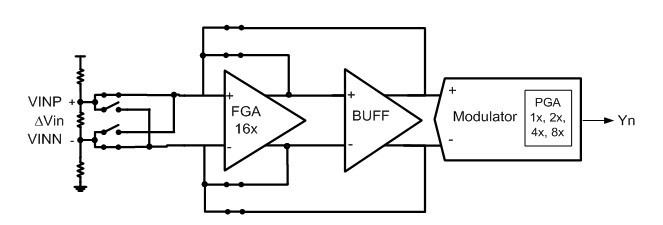
    Gain calibration for the PGA (programmable gain amplifier, 1x – 8x) in the modulator is done by bypassing the FGA (fixed gain amplifier) and the buffer blocks, as shown in the figure.  Alternate samples, DVin and -DVin, at a known voltage are obtained. Then, the PGA gain coefficient, G’pga, is obtained by dividing the difference of alternate ADC outputs by the difference of alternate samples, as shown in the equation. The digital output code is multiplied by G’gpa to correct for the PGA error.

    G'pga = (Y2-Y1)/(-2dVin)

    The input is alternated so that the offset does not affect the gain calibration.

    Mike