This thread has been locked.

If you have a related question, please click the "Ask a related question" button in the top right corner. The newly created question will be automatically linked to this question.

Interfacing ADS5400 with Virtex 6 via a FMC-ADC adapter

Other Parts Discussed in Thread: ADS5400, ADS62P49, FMC-ADC-ADAPTER, ADS5483

Hi,

Can you please describe what are the steps involved for interfacing a TI ADS5400 with parallel LVDS output to the Virtex 6 FPGA via a FMC-ADC adapter? I browsed the forum, and it seems that all the relevant information points to the serial LVDS output from other lines of TI ADC cards. I understand that for serial LVDS output, we must have a Deserializer implemented in FPGA fabric.

What about the 12-bit LVDS parallel output? Do I just need to specify the correct IOSTANDARD for the pins on the FMC connector of Virtex 6, and the 12-bit data will be automatically buffered correctly?

I appreciate your help in this matter.

Best Regards,

Danh.

  • Hi,

    I can describe how we interfaced the ADS5400 LVDS data to the Virtex4 on our TSW1200 capture card.   Please see the attached sketch which illustrates the input circuit in the FPGA.

    We bring the DDR clock and the data lines into an LVDS input buffer with the 100 ohm termination resistor in the FPGA enabled.  Then each LVDS line, both clock and data, pass through an IDELAY element.  This lets us individually skew the clock and/or the data to meet setup time into whatever is used to latch the data.

    The clock has to pass through a clock buffer, so the data had an IDELAY setting to make the data path match the clock path with regards to timing.  Then we used an IDDR cell to latch the data on the rising edge and falling edge, while reregistering the falling edge data over to the rising edge.  At this point, the sample data is ready to be used in the FPGA for whatever you wish to do with it.

    On the TSW1200, we chose to use the ADS5400 in dual bus mode, so there are more LVDS data channels that i had initally indicated in the attached file.  I use in fact 24 LVDS inputs and clock at 500Mbps.  But the Virtex 4 is fast enough that i *could* have operated in single bus mode for 12bits of data at 1000Mbps using the same logic in the FPGA (the input buffer, IDELAY and IDDR).

    The IO standard for the input buffer was just LVDS_25 as in this code from my constraints file:


    NET "D0_p_pin" LOC = "A16" | IOSTANDARD = "LVDS_25";

    NET "D0_n_pin" LOC = "B16" | IOSTANDARD = "LVDS_25";

    and


    INST "IBUFDS_inst00" IOSTANDARD="LVDS_25";

    and for the termination resistor

    INST "IBUFDS_inst00" DIFF_TERM = TRUE;

    And for meeting the timing of the setup and hold (finding the right settings for the IDELAY) we take our best guess at what the IDELAY deafult tap settings should be and set that as default powerup or reset IDELAY values.  Then we check the static timing analysis report after place and route, looking for timing violations.  If there is a timing violation on the DDR input data, then we look at the magnitude of the violation and that tells us how many IDELAY tap settings we were off by on our initial guess.  Then we rerun the timing tools to verify.  (This all presumes that you have the timing constraints entered into the ucf file to describe the clock rate and the setup and hold timing from the ADS5400 data sheet properly.  This is not trivial - i always found this particular step to be less than obvious to get done correctly.)

    And since you are using the adapter card into a Xilinx development platform, you will need to enter in the ucf file the pin number that each LVDS signal is to be found on for the FPGA in question.  (You'll need the mapping from FMC to FPGA for your particular development platform.)

    Regards,

    Richard P.

  •  

    Hello Richard Prentice,


    first of all, thank you for all informations you published about interfacing adc with fpga's...


    I have the TSW1200 and ADS62P49 (250 MSPS) as well...

    My first fpga configuration was a ddr-sdr-converter and fifo with rs 232 interface to send the adc data to the pc. The first ddr-sdr-converter has been programmed by my self (without IDDR). This configuration works correctly with a sample frequency of 25 MHz. When I set the adc sample frequency to 250 MHz it doesnt work - but this is not a miracle - for 250 MHz I have to use the IDDRs.

    So I deleted my self written ddr-sdr-converter and insert IDDRs with IDELAY before... I set the timing constraints and set the idelay so that the timing of the design get met as you described ...   But neither with 25 MHz nor 250 MHz the IDDRs works correctly... see the image below...


    I guess that there is a synchronization problem - see image below - the clock and ddr-data come synchronous into the fpga and go through the IDELAY elements. The timing constraints and report says that everything is ok. But I dont know if the timing constraints cover the path thrugh the BUFR and IDDR... I guess that the data flow faster through the IDDRs than throgh the BUFR and so the fifo that is direct driven by the CLK_ADC and the data ADC_SDR_A(x) is not anymore synchronous... ??? My timing constraint are:

    # ADS62P49 connection port A
     
    NET "DA0M"     LOC = B16 | IOSTANDARD = LVDS_25 | DIFF_TERM = TRUE | TNM = ADC_Input;
    NET "DA0P"    LOC = A16 | IOSTANDARD = LVDS_25 | DIFF_TERM = TRUE | TNM = ADC_Input;

    NET "DA2M"    LOC = A15 | IOSTANDARD = LVDS_25 | DIFF_TERM = TRUE | TNM = ADC_Input;
    NET "DA2P"    LOC = B15 | IOSTANDARD = LVDS_25 | DIFF_TERM = TRUE | TNM = ADC_Input;

    .........................


    # ADS62P49 ADC-DDR-Clock

    NET "CLK_ADC_M"    LOC = B19 | IOSTANDARD = LVDS_25 |  DIFF_TERM = TRUE;
    NET "CLK_ADC_P"     LOC = C20 | IOSTANDARD = LVDS_25 |  DIFF_TERM = TRUE;

    NET "CLK_ADC_M"     TNM_NET = CLK_ADC_M;
    TIMESPEC TS_CLK_ADC_M = PERIOD "CLK_ADC_M" 250 MHz HIGH 50 %;
    NET "CLK_ADC_P"     TNM_NET = CLK_ADC_P;
    TIMESPEC TS_CLK_ADC_P = PERIOD "CLK_ADC_P" 250 MHz HIGH 50 %;

    TIMEGRP "ADC_Input" OFFSET = IN 0.9 ns VALID 1.85 ns BEFORE "CLK_ADC_M" RISING;
    TIMEGRP "ADC_Input" OFFSET = IN 0.9 ns VALID 1.85 ns BEFORE "CLK_ADC_M" FALLING;

    TIMEGRP "ADC_Input" OFFSET = IN 0.9 ns VALID 1.85 ns BEFORE "CLK_ADC_P" RISING;
    TIMEGRP "ADC_Input" OFFSET = IN 0.9 ns VALID 1.85 ns BEFORE "CLK_ADC_P" FALLING;


    Do you have a hint for me or do you know the failure I do??

  •  

    Problem solved!


    The problem was, that the adc-ddr-clock is connected wrong to the fpga-lvds-input-clock-pins: the p site is connected to the n site and the n to the p site -> so, the adc-ddr-clock comes into the fpga inverted. Because there is no opportunity in the io-logic to invert the incoming clock - I had to change the outputs of the IDDR primitive and use it in the OPPOSITE_EDGE mode (SAME_EDGE_PIPELINED is not possible because of the inverted clock!!!).

    The wrong data consists of the inverted clock - the data that comes out of the IDDR is not valid with the rising ege of the clock signal - it is valid with the falling edge and changes again with the rising edge!!!

     So I insert a buffer that buffers the incoming data by the IDDR with every falling clock edge and so the fifo can take the data with the rising clock edge...


  • Hello, Richard,

    I came into the Forum before with a question about using the ADS5483EVM  without a PC interface, to which I got a response, and which I appreciated. *Long* before my post relative to the EVM our plan was to simulate operation of a receiver by using the combination of the EVM with a Virtex-6 ML605 board. By a real stroke of luck, I was able to find the FMC-ADC-Adapter (I have Rev. C) which solved a whole host of problems, as I initially thought I was going to have to fabricate an interface cable and didn't know how I was going to be able to efficiently account for varying cable lengths. Over the course of the project I've absolutely scoured every piece of information/application note that I could get my hands on relative to the LVDS interface, and have found your descriptions here very informative and practical. While I have done quite a bit of ADC/uP interfaces, I've never had to do one which operates at these speeds, i.e., 100+ MSPS, or with a differential data stream. I do have a few questions:

    1 - Signal (pin) names on the FNC end of the adapter are exactly opposite the pin names on the ADC end, i.e., D8_D9_P ====>IO_7N

                                                                                                                                                                                                            D8_D9_M ====>IO_7P

    should these be reversed in the FPGA pin assignments ? I.e., even though I have IO_7N, should I just connect this to i.e., FMS_LPC_LA19_P, as this was the polarity that the original signal started out with (not worried so much about the pin #, the issue is whether reverse the signal 'polarity' when doing the FPGA pin assignments) ? This is the same situation with the clock signals.


    2 - From your diagram, i.e., 'IBUFDS' to 'IDELAY' to 'IDDR', it seems I need to follow IDDR with two banks of FF's to either:

                       a - utilize one bank to capture even and odd data for bits (0, 2,...14) and one bank to capture even and odd data for bits (1,2,...., 15)

                  or, b - follow each 'IDDR' block by a conversion to magnitude, and latch up the magnitude data

        Am I close ??


    3 - Though the MicroBlaze is the processor I have in mind (running the ADS5473 at 120 MSPS), did you all use interrupt processing to handle the data acquisition in the TSW1200 ?


    4 - Would like to take you up on the previously stated offer (in a different post) of TSW1200 (code/Verilog). Is there a way to get you my email without posting it to the forum ?


    Thanks,

    Jim


  • Hello Jim,

    I'm not Richard indeed, but I can almost answer all of your questions...

    to question 1:

    I recommend to you to check the pin assignment. At my eval. board (ADS62P49) the adc data bus names were correct but the clock was inverted... To safe time it's better to check everything.... You have to connect the positiv data pin from the adc to the positiv pin of the fpga!!!

    to question 2:

    IBUFDS and IDELAY are in the design to read in the adc dual data rate data (on the one ege the odd bits and the other edge the even bits). To convert the dual data rate data you have to use the IDDRs. The IDDRs are discribed in the user guide of the fpga you are using - for example http://www.xilinx.com/support/documentation/user_guides/ug070.pdf page 323. You can run the IDDRs in three different modes - see user guide.... The data that comes out of the IDDR is in single data format and useable for your fpga design (the IDDRs convert a ddr-data-bus with n bits into a sdr-data bits with 2 * n bits)...

    to question 3:

    In the TSW1200 design is no soft core processor... There is only a fifo and a state machine.... I think it is not a good way to process the adc data with a soft core... Store the samples you need in a asynchonous fifo and then you can load the data into the soft core with a lower clock that comes out of the soft core...

    to question 4:

    I' dont know.... But if you provide your mail adress i can send you the files...


    Regards S.D.


  • Hello, Simon,


    To question/answer #1 - I had already checked the pin assignment; the second part of your answer was the more informative, i.e., pos.-to-pos., neg.-to-neg. which overcomes any disparity in signal labeling on the various boards as mentioned in my original post.

    To question/answer#2 - I've already looked in the User's Guide and understand the basics of DDR data, and the three different modes. The specific question has to do with the fact that the ADS5483 has not only DDR data, but multiplexed DDR data, hence my question about latches, because on CLK_P/CLK_N you get even/odd data for the first data word, i.e., for D0, (....D2,D4,...,D14) on the next CLK_P/CLK_N transition you get D1(..., D3, D5,..., D15), i.e., the second set of data on the multiplexed line.

    To question/answer#3 - We've already considered using FIFO's. Due to the nature, i.e., size, of the data which must be captured before *any* processing can begin none of the configurations available from the Xilinx IP Generator will work, which leaves us with trying to kluge/string a bunch of smaller FIFO's together with some glue logic, or writing a Verilog or software version.

    Thanks,

    Jim


  • Good morning...

    to your question / answer #2:

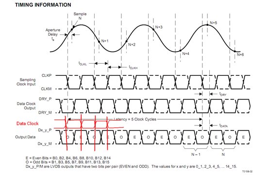
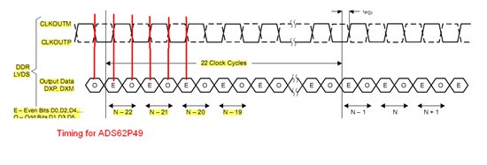
    the data is not realy multiplexed - it' is in a dual data rate format... As you can see below there is the timing information of the ADS5483 and ADS62P49 (both use ddr as output).

    The difference between the two timing diagramms is, that in the timing of ADS5483 the clock and data is in phase and because of this you cant say the data is valid with the positive or negative edge...

    In the timing of the ADS62P49 you can see that the even bits are valid with the positive edge of "CLKOUTP"  and  the odd bits with the negative edge of  "CLKOUTP...I use the ADS62P49 and can confirm the timing diagram....

    So I think there is either a failure in the timing diagramm of the ADS5483 or the timing diagramm is right and you have to delay the clock within the fpga and then drive the IDDRs... and this question shoud be answered by somebody of TI...


    Timing of the ADS5483

    in red you can see how the clock shoud be for a source synchronous design...


    Timing of the ADS62P49

    To question/answer#3 : what exactly are you planning to do?


    Regards S. D.


  • Hi,

    Wow, after all this time i just came across  the postings to this thread since i last posted to it.  I think because the thread was marked as 'answered' that the further postings did not get copied to me, so i never saw them.

    The timing for the ADS5483 is indeed what is is often called source-synchronous, where the clock edge is aligned with data transitions.  This does mean that there must be some delay function on the receiving side to position the clock edge such that the data can be latched in.  This is a common interface in some circles, as i have often seen it in the interface between SERDES devices and an ASIC, for example.  FPGAs are usually quite capable of handling such an interface.

    The timing of the ADS62P49 is in contrast a source-centered format.

    It turns out with the Virtex4 of the TSW1200 that a delay function was required to meet setup and hold time into the IDDR cells for both devices. Even with the case where the clock was centered on the data valid out of the ADC the clock buffering into the FPGA skewed the clock anyway - making a recentering necessary.  Neither format was better or worse for meeting setup and hold time into the FPGA - just different delay settings were needed.

    Regards,

    Richard P.

  • Hi,

    I am trying to implement the necessary code in order to connect ADS5400 and Virtex 6. I tried with the schemes posted by Richard and Simon, i.e.:

    -13 IBUFDS blocks (12 data + 1 clock)

    -13 IDElAY blocks

    -1 BUFIO block

    -1 BUFR block

    -12 IDDR blocks

    When I try to implemt the design I have this error map:

    LIT:534 - BUFIODQS symbol "BUFIO_inst_clock" (output signal=clock_bufio)
       cannot drive a BUFR. Please modify your design to avoid this unroutable
       situation.

    Can I connect directly BUFIO and BUFR? This is a difference between both of schemes, Richard doesn't use BUFR and Simon does. I'm not sure if I must use this block. If I delete BUFR I have the next two errors:

    Place:1362 - IO Clock Net "clock_bufio" drives a load pin on a component
       ("clock_bufio_out_OBUF" type-LUT) that is not on any IO column.
       To debug your design with partially routed design, please try to allow
       map/placer to finish the execution (by setting environment variable
       XIL_PAR_DEBUG_IOCLKPLACER to 1).

    Pack:1654 - The timing-driven placement phase encountered an error.

    If you think it is neccesary, I will post the code, but I can comment the more particular things now:

    -About IBUFS, I obtain the same result using generic map or not :

    --generic (IOSTANDARD : string := "LVDS_25"; IFD_DELAY_VALUE: string := "0"; DIFF_TERM: boolean := FALSE) 

    -Is this ok?

    -About IDELAY, at the beginning I am using DEFAULT mode. I think I will need the FIXED or VARIABLE modes, but I don't know exactly how I can instantiate the IDELAYCTRL. Could you tell me how can I do?

    -About IDDR I am using this generic map:  DDR_CLK_EDGE => "OPPOSITE EDGE", INIT_Q1 => '0', INIT_Q2 => '0', SRTYPE => "SYNC".

    Thanks a lot for your help,

    Jose


  • HI Simon, i am doing the same, can you share the above written code with me. it would really appreciated.

    Thanks
  • Hi,

    I am not Simon, and could not share Simon's solution because I do not have it.  I have on this forum sent the TSW1200 Virtex 4 code when asked, and when provided with an email address to send it to. 

    Since this posting thread hops around from different ADC EVMs to different FPGAs being used and different problems encountered, in general it would have been best for the different posters to start new threads so that each thread could been about a specific issue.

    One issue that Simon mentioned was due to polarity of the LVDS clocking.  For our LVDS-format EVMs we would often instruct the layout person to construct the EVM with the cleanest LVDS pair layout to the connector, avoiding vias through the board to swap pairs.  If this meant that the LVDS pair for either clock or data ended up being swapped between plus and minus, then we would deal with that in the FPGA code of the older TSW1200 (based around the Xilinx Virtex4) or the newer TSW1400 (based around an Altera Stratix).  It is easy to deal with, if you know that that may be a problem.  So when bringing the EVM into an FPGA development platform, that polarity would indeed have to be something to be checked out up front.  But since the clocking is dual data rate, an inverted clock just means that the bits you were looking for on rising edge end up being on falling edge and vice versa.

    Other issues brought up in this old posting dealing with Xilinx compilation errors and what buffers are allowed to drive what loads - that would have had to have been addressed in a Xilinx forum. 

    Regards,

    Richard P.

  • Thanks Richard for the reply, let me start a new thread for my new issues, and will discuss with you there...