This thread has been locked.

If you have a related question, please click the "Ask a related question" button in the top right corner. The newly created question will be automatically linked to this question.

ADS8568: No Response from the ADC

Part Number: ADS8568
Other Parts Discussed in Thread: TM4C123GH6PM

Hi,

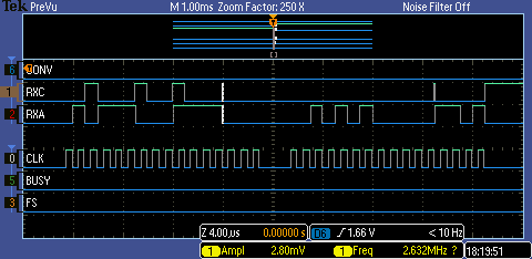
This is my first thread here.  I'm having trouble setting up my ADS8568 in SW mode. I'm using serial interface, and just trying to start conversion and reading data from the ADC.

I'm running the master device TM4C123GH6PM microcontroller.

To verify that my ADC is soldered to my breakout board correctly, I'm seeing about 0.001mA from my Multimeter.

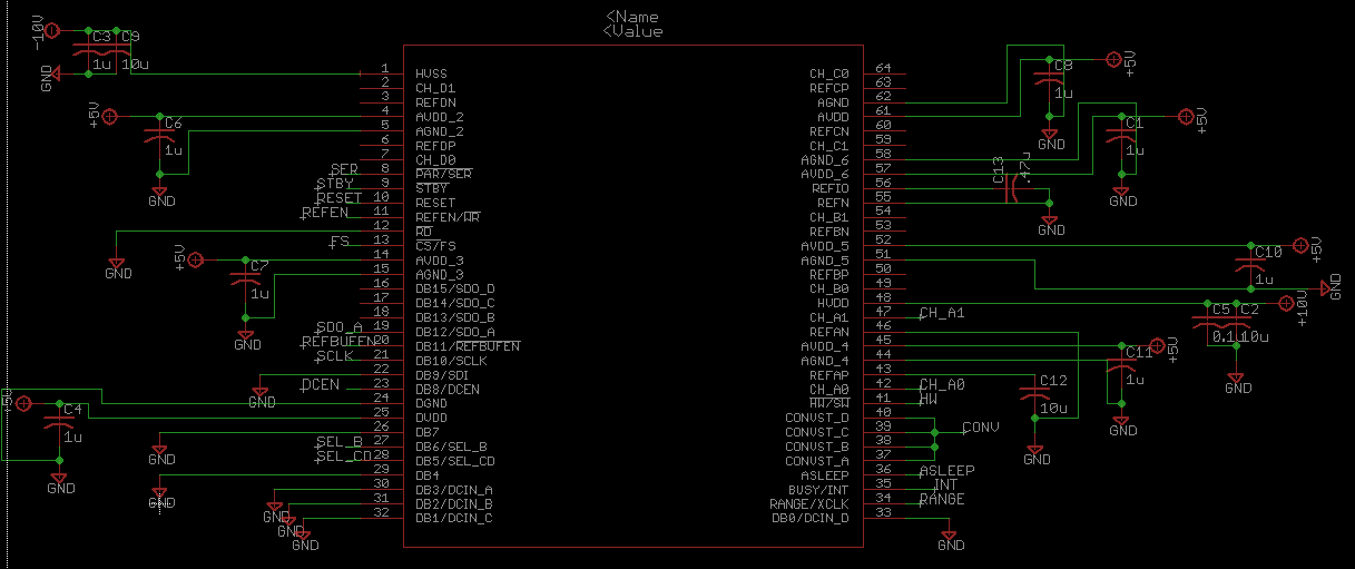
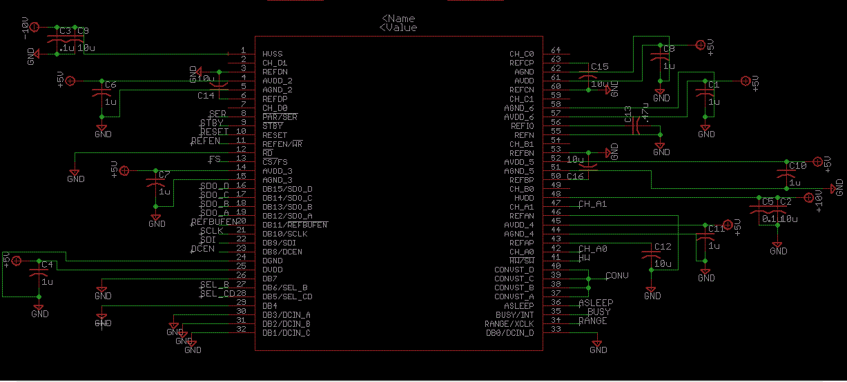
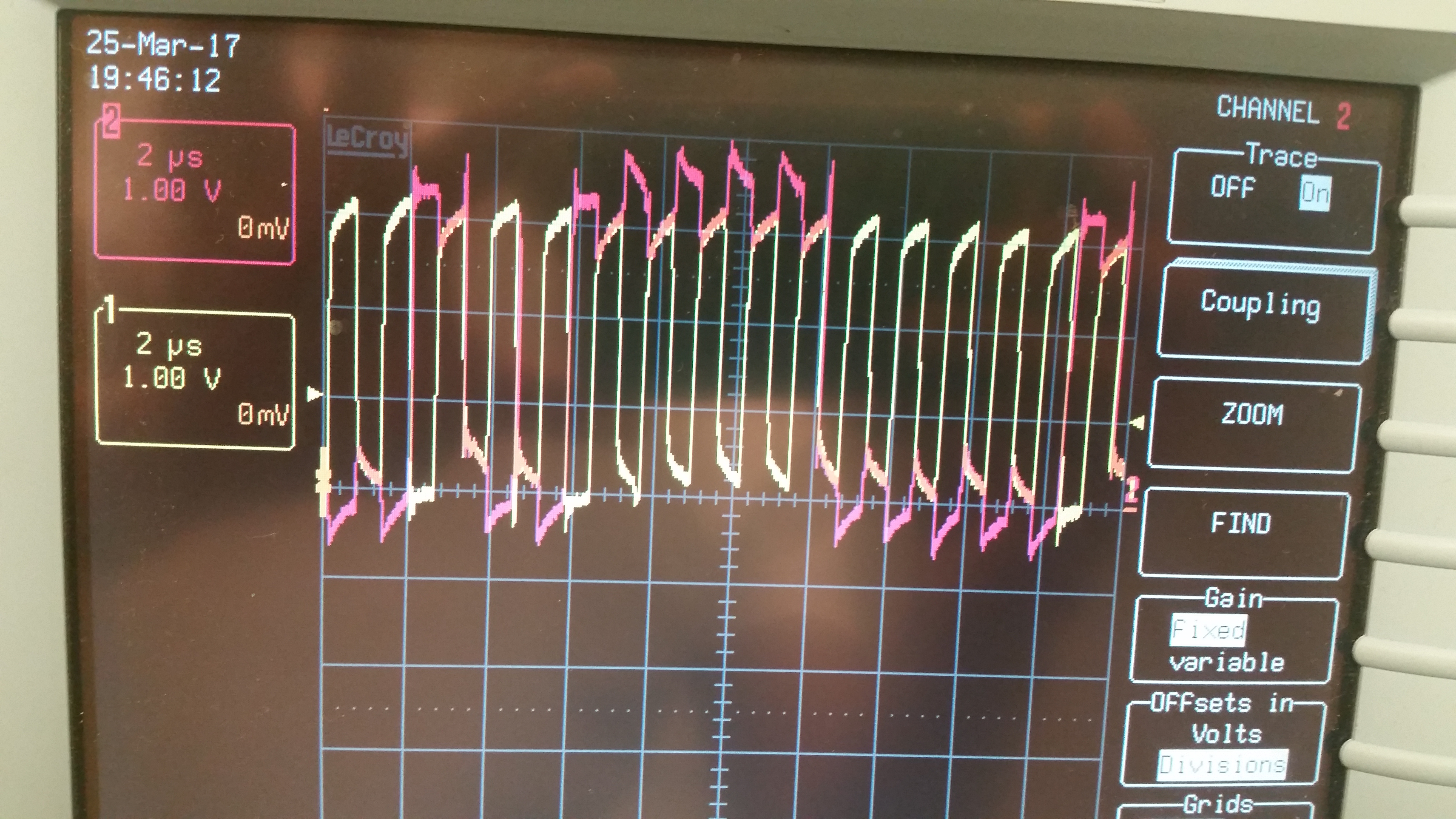
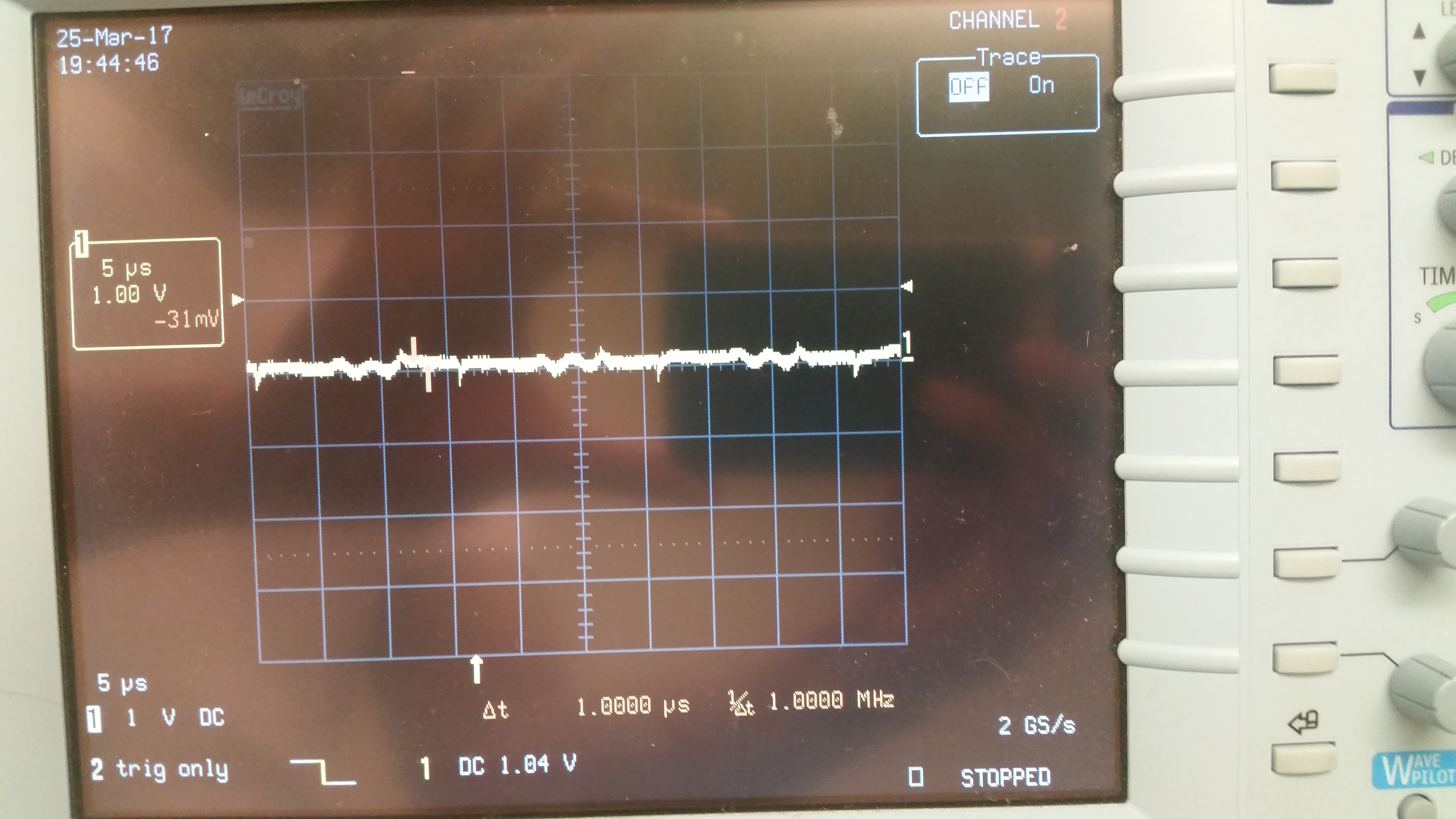
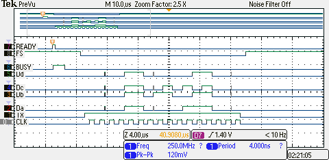
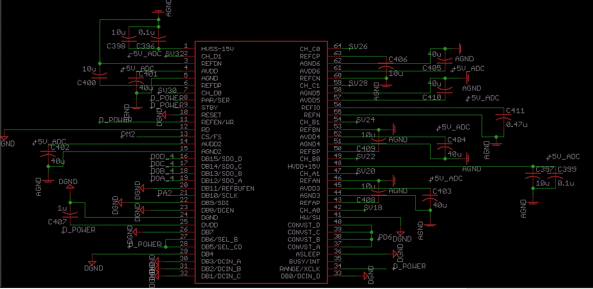
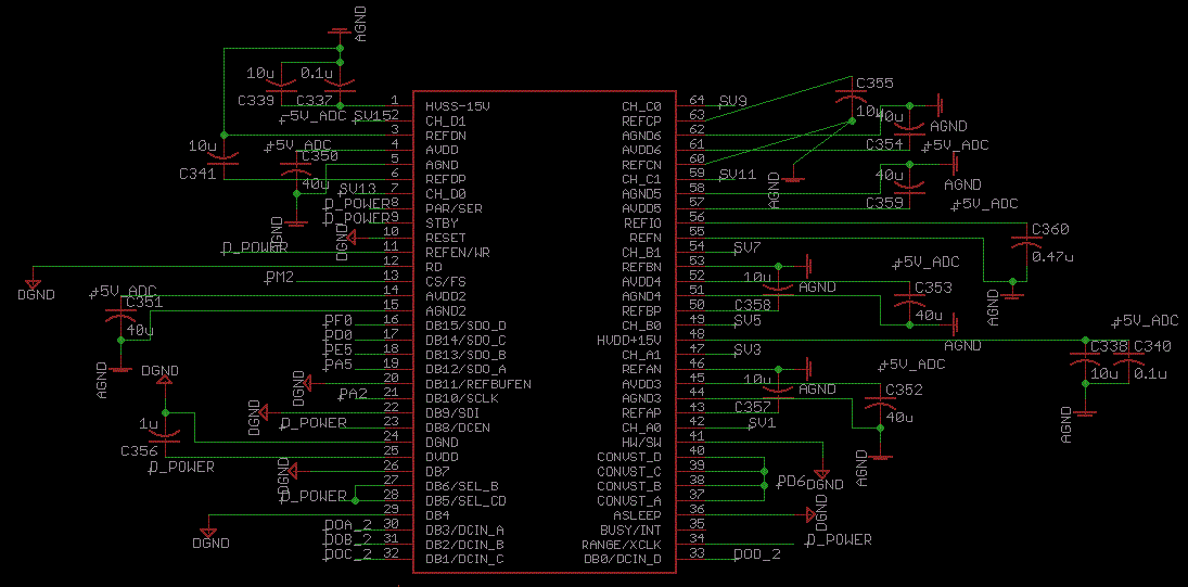
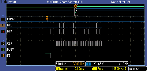
Please see code and my schematic. Thanks.

-Ianadc8668_sch.sch

#include <stdint.h>
#include <stdbool.h>
#include "driverlib/sysctl.h"
#include "driverlib/uart.h"
#include "driverlib/ssi.h"
#include "driverlib/cpu.h"
#include "utils/uartstdio.h"
#include "inc/hw_memmap.h"
#include "inc/tm4c123gh6pm.h"

#define NUM_SSI_DATA            3
#define SSI0 0x3C // SSI PA2,PA3,PA4,PA5
/*
PA2 - SSI0Clk
PA3 - SSI0Fss
PA4 - SSI0Rx
PA5 - SSI0Tx

*/
uint32_t data32;

void PortAInit() {
	SYSCTL_RCGC2_R |= SYSCTL_RCGC2_GPIOA;
	SYSCTL_RCGC1_R |= SYSCTL_RCGC1_SSI0; // enable SSI0 module
	SysCtlDelay(1);
	
	GPIO_PORTA_AFSEL_R |= 0x3C; // SSI0 pins
	GPIO_PORTA_PCTL_R |= 0x222200; // SSI0Tx, SSI0Rx, SSI0Fss, SSI0CLK
	GPIO_PORTA_DEN_R |= 0x7C; // PA2 - PA6
	GPIO_PORTA_AMSEL_R &= ~0x7C; // disabled analog

	// SSI clock = system clk / (CPSR * (SCR+1))
	SSI0_CR1_R = 0x10; // disable SSI0 and Master mode
	SSI0_CC_R = 0x00; // use system clock for SSI0
	SSI0_CPSR_R = 0x2; // Clock Prescale 2
	SSI0_CR0_R |= 0x91F; // SCR = 9, TI frame format, 16-bit data. Bit-rate = 1MBPS
	
	SSI0_IM_R |= 0x0C; // receive FIFO and EOT interrupt unmasked
	NVIC_EN0_R = (0x1 << 7); // NVIC enable SSI0
	NVIC_PRI1_R |= (0x1 << 29); // NVIC priority 1 SSI0
	
	SSI0_CR1_R |= 0x02; //enable SSI0
}

void PortEInit() {
	SYSCTL_RCGC2_R |= SYSCTL_RCGC2_GPIOE;
	GPIO_PORTE_DEN_R |= 0x3F; // digital
	GPIO_PORTE_DIR_R |= 0x3D; // output 0011_1101
	GPIO_PORTE_DIR_R &= ~0x02; // input PE1
	GPIO_PORTE_AFSEL_R &= ~0x3F;	// gpio
	
	GPIO_PORTE_IS_R &= ~0x02; // edge-sensitive
	GPIO_PORTE_IBE_R |= 0x02; // both edge
//	GPIO_PORTE_IEV_R &= ~0x02; // active low edge
	GPIO_PORTE_ICR_R |= 0xFF; // clear any pin interrupt
	GPIO_PORTE_IM_R |= 0x02; // unmask (enable) interrupt
	
	NVIC_EN0_R = (0x1 << 4); // NVIC enable GPIOPortE
	NVIC_PRI1_R |= (0x2 << 5); // NVIC priority 2 GPIOPortE
}

void PortFInit() {
	SYSCTL_RCGC2_R |= SYSCTL_RCGC2_GPIOF;
	SysCtlDelay(1);
	
	GPIO_PORTF_LOCK_R = 0x4C4F434B;
	GPIO_PORTF_CR_R |= 0x01;	// allow changes to PF0
	GPIO_PORTF_DEN_R |= 0x1F; // digital
	GPIO_PORTF_DIR_R |= 0x0E; // output
	GPIO_PORTF_PUR_R |= 0x11;	//pull up resistor
	
	GPIO_PORTF_IS_R &= ~0x11; // edge-sensitive
	GPIO_PORTF_IBE_R |= 0x11; // both edge
//	GPIO_PORTF_IEV_R &= ~0x01; // active low edge
	GPIO_PORTF_ICR_R |= 0x11; // clear any pin interrupt
	GPIO_PORTF_IM_R |= 0x11; // unmask (enable) interrupt
	
	NVIC_EN0_R = (0x1 << 30); // NVIC enable GPIOPortF
	NVIC_PRI7_R |= (0x2 << 21); // NVIC priority 2 GPIOPortF
}

void GPIOE_Handler () {
	uint16_t dout;
	GPIO_PORTE_ICR_R = 0x02;
	
	if(GPIO_PORTE_RIS_R & 0x02){
		GPIO_PORTA_DATA_R |= 0x08; // Set pin to HIGH
		GPIO_PORTF_DATA_R |= 0x04; // LED green ON
		SysCtlDelay(6666666); // 1s
		GPIO_PORTF_DATA_R &= ~0x04; // LED green OFF
		GPIO_PORTA_DATA_R &= ~0x08; // FS triggered
	}
		if (SSI0_RIS_R & 0x04){
		dout = SSI0_DR_R;
		while(SSI0_SR_R & 0x10);
		
		UARTprintf("Value: %d\n", dout);
	}
	UARTprintf("ADC Busy received");
}


void GPIOPortFHandler(void) {
		NVIC_DIS0_R = (0x1 << 30);   //disable interrupt Port F
		SysCtlDelay(41667);
	//DELAY = desired delay (s) * system clock / 3
	
		// Control frame select
		if(GPIO_PORTF_RIS_R & 0x01) { // switch 2 pressed
		// acknowledge PF0
		GPIO_PORTF_ICR_R = 0x01;
			
//		GPIO_PORTA_DATA_R |= 0x08; // SSI0 Fss HIGH
		GPIO_PORTE_DATA_R |= 0x01; // FS High
		GPIO_PORTF_DATA_R |= 0x04; // pressed
		SysCtlDelay(6666666); // 1s
		GPIO_PORTF_DATA_R &= ~0x04; // released
		GPIO_PORTE_DATA_R &= ~0x01; // FS LOW
//		GPIO_PORTA_DATA_R |= 0x08; // SSI0 Fss HIGH

//		GPIO_PORTA_DATA_R &= ~0x08; // Falling edge triggered
		
		data32 = SSI0_DR_R;	
		while(SSI0_SR_R & 0x10) {}; // wait for serial data shift done
		UARTprintf("Data: \n");
		UARTprintf("%d", data32);
		}
		
		// ready to convert
		if(GPIO_PORTF_RIS_R & 0x10) { // switch 1 pressed
		// acknowledge PF4
		GPIO_PORTF_ICR_R = 0x10;
		
		GPIO_PORTA_DATA_R &= ~0x40;	// Set CONV pin to LOW
		
		GPIO_PORTF_DATA_R |= 0x08; // Green ON
		SysCtlDelay(6666666); // 1s
		GPIO_PORTF_DATA_R &= ~0x08; // Green OFF	
		GPIO_PORTA_DATA_R |= 0x40;	// Convert
		SysCtlDelay(6);
		GPIO_PORTA_DATA_R &= ~0x40;	// Set pin to LOW			
		}
		
		NVIC_EN0_R = (0x1 << 30);    //reenable interrupt port F
}
void SSI0_Handler() {
	uint16_t dout;
	
	if (SSI0_RIS_R & 0x04){
		dout = SSI0_DR_R;
		while(SSI0_SR_R & 0x10);
		
		UARTprintf("Value: %d\n", dout);
	}
	
	if (SSI0_RIS_R & 0x08){
		GPIO_PORTE_DATA_R |= 0x01; // FS HIGH
		UARTprintf("Tx is empty\n");
	}
	
}

void ConfigureUART() {
	SYSCTL_RCGC2_R |= SYSCTL_RCGC2_GPIOA;
	SYSCTL_RCGC1_R |= SYSCTL_RCGC1_UART0;

	// Configure GPIO Pins for UART mode.
	GPIO_PORTA_DEN_R |= 0x3;	//digital
	GPIO_PORTA_AFSEL_R |= 0x3;	//uart function
	GPIO_PORTA_PCTL_R |= 0x11;	//UART PA1,PA0

	UART0_CC_R = 0x5;	//PIOSC source 16MHz

	//
	// Initialize the UART for console I/O.
	//
	UARTStdioConfig(0, 115200, 16000000);
}

int main(void) {
	
	CPUcpsid();	// Disable interrupts globally.
	SysCtlClockSet(SYSCTL_SYSDIV_10 | SYSCTL_USE_PLL | SYSCTL_XTAL_16MHZ | SYSCTL_OSC_MAIN); // system clock 20MHz
	
	PortAInit();
	PortEInit();
	ConfigureUART();
	PortFInit();
	
	{
	CPUcpsie();	// Enable interrupts globally	
		
		GPIO_PORTE_DATA_R |= 0x0C; // PE2(SW), PE3(SER)
		GPIO_PORTE_DATA_R &= ~0x30; // PE4(SEL_B), PE5(SEL_CD)	
		
		GPIO_PORTE_DATA_R |= 0x01; // FS High
		SSI0_DR_R = 0x0054; // ADC Configuration bits
		while(SSI0_SR_R & 0x10) {}; // wait for serial data shift done
//		GPIO_PORTA_DATA_R |= 0x08; // PortA Fss high
			
		SSI0_DR_R = 0x0000; // ADC Configuration bits
		while(SSI0_SR_R & 0x10) {}; // wait for serial data shift done
		GPIO_PORTE_DATA_R &= ~0x01; // FS LOW
	  SysCtlDelay(100);
		GPIO_PORTE_DATA_R |= 0x01; // FS HIGH
							
	}
	
	while(1) {
//		GPIO_PORTA_DATA_R |= 0x08; // PortA Fss high
//		SSI0_DR_R = 0xA00A; // ADC Configuration bits
//		while(SSI0_SR_R & 0x10) {}; // wait for serial data shift done
//		GPIO_PORTE_DATA_R |= 0x01; // FS High
//		SSI0_DR_R = 0x8054; // ADC Configuration bits
//		while(SSI0_SR_R & 0x10) {}; // wait for serial data shift done
////		GPIO_PORTA_DATA_R |= 0x08; // PortA Fss high
//			
//		SSI0_DR_R = 0x0000; // ADC Configuration bits
//		while(SSI0_SR_R & 0x10) {}; // wait for serial data shift done
//		GPIO_PORTE_DATA_R &= ~0x01; // FS LOW
	}
}

  • Hello Ian,

    Could you please clarify how you checked the current to verify if ADS8568 is soldered correctly? What's the meaning of "No response from the ADC?" also your uploaded schematic is empty after checked, please verify. Thanks.

    Best regards

    Dale Li

  • I hooked up my ADC8568 with an ammeter from my power supply (~5V). At the moment, I'm reading ~46mA while not doing any conversion (idle).

    So I think my ADC is at least working...

    Please see my code and schematic. I setup an Interrupt to read from the BUSY pin of ADC, and it goes HIGH by reading the Status register of uController.

    However, when I'm trying to read the output from Channel A, I'm reading 0. I'm reading from a potentiometer just as a test.

    To read from the ADC, I use GPIO pin that goes from HIGH to LOW when I'm about to read it, then it goes back HIGH again.

    Update and Additional info. I'm now using Hardware mode, TM4C123GH6PM microcontroller, and the schematic below represents my breakout board which is connected (jumper wired) to my microcontroller.

    #include <stdint.h>
    #include <stdbool.h>
    #include "driverlib/sysctl.h"
    #include "driverlib/uart.h"
    #include "driverlib/ssi.h"
    #include "driverlib/cpu.h"
    #include "utils/uartstdio.h"
    #include "inc/hw_memmap.h"
    #include "inc/tm4c123gh6pm.h"
    
    #define SSI0 0x3C // SSI PA2,PA3,PA4,PA5
    /*
    PA2 - SSI0Clk
    PA3 - SSI0Fss
    PA4 - SSI0Rx
    PA5 - SSI0Tx
    
    */
    uint32_t data32;
    
    void PortAInit() {
    	SYSCTL_RCGC2_R |= SYSCTL_RCGC2_GPIOA;
    	SYSCTL_RCGC1_R |= SYSCTL_RCGC1_SSI0; // enable SSI0 module
    	SysCtlDelay(1);
    	
    	GPIO_PORTA_AFSEL_R |= 0x3C; // SSI0 pins
    	GPIO_PORTA_PCTL_R |= 0x222200; // SSI0Tx, SSI0Rx, SSI0Fss, SSI0CLK
    	GPIO_PORTA_DEN_R |= 0xFC; // PA2 - PA7
    	GPIO_PORTA_DIR_R |= 0xEC; // output
    	GPIO_PORTA_DIR_R |= 0x10; // input
    	GPIO_PORTA_AMSEL_R &= ~0xFC; // disabled analog
    
    	// SSI clock = system clk / (CPSR * (SCR+1))
    	SSI0_CR1_R = 0x10; // disable SSI0 and Master mode, EOT active
    	SSI0_CC_R = 0x00; // use system clock for SSI0
    	SSI0_CPSR_R = 0x2; // Clock Prescale 2
    	SSI0_CR0_R |= 0x90F; // SCR = 9, Freescale frame format, 16-bit data. Bit-rate = 1MBPS
    	
    	SSI0_IM_R |= 0x00; // receive FIFO and EOT interrupt unmasked
    	NVIC_EN0_R = (0x1 << 7); // NVIC enable SSI0
    	NVIC_PRI1_R |= (0x1 << 29); // NVIC priority 1 SSI0
    	
    	SSI0_CR1_R |= 0x02; //enable SSI0
    }
    
    void PortCInit() {
    	SYSCTL_RCGC2_R |= SYSCTL_RCGC2_GPIOC;
    	
    	GPIO_PORTC_DEN_R |= 0x70; // PC4, PC5, PC6
    	GPIO_PORTC_DIR_R |= 0x70; // output
    }
    
    void PortDInit() {
    	SYSCTL_RCGC2_R |= SYSCTL_RCGC2_GPIOD;
    	GPIO_PORTD_DEN_R |= 0x40; // PD6
    	GPIO_PORTD_DIR_R |= 0x40;
    }
    
    void PortEInit() {
    	SYSCTL_RCGC2_R |= SYSCTL_RCGC2_GPIOE;
    	GPIO_PORTE_DEN_R |= 0x3F; // PE0 - PE5
    	GPIO_PORTE_DIR_R |= 0x3D; // output 0011_1101
    	GPIO_PORTE_DIR_R &= ~0x02; // input PE1
    	GPIO_PORTE_AFSEL_R &= ~0x3F;	// gpio
    	
    	GPIO_PORTE_IS_R &= ~0x02; // edge-sensitive
    	GPIO_PORTE_IBE_R &= ~0x02; // rise edge only
    	GPIO_PORTE_IEV_R |= 0x02; // active rise edge
    	GPIO_PORTE_IM_R |= 0x02; // unmask (enable) interrupt
    	
    	NVIC_EN0_R = (0x1 << 4); // NVIC enable GPIOPortE
    	NVIC_PRI1_R |= (0x2 << 5); // NVIC priority 2 GPIOPortE
    }
    
    void PortFInit() {
    	SYSCTL_RCGC2_R |= SYSCTL_RCGC2_GPIOF;
    	SysCtlDelay(1);
    	
    	GPIO_PORTF_LOCK_R = 0x4C4F434B;
    	GPIO_PORTF_CR_R |= 0x01;	// allow changes to PF0
    	GPIO_PORTF_DEN_R |= 0x1F; // digital
    	GPIO_PORTF_DIR_R |= 0x0E; // output
    	GPIO_PORTF_PUR_R |= 0x11;	//pull up resistor
    	
    	GPIO_PORTF_IS_R &= ~0x11; // edge-sensitive
    	GPIO_PORTF_IBE_R |= 0x11; // both edge
    	GPIO_PORTF_IM_R |= 0x11; // unmask (enable) interrupt
    	
    	NVIC_EN0_R = (0x1 << 30); // NVIC enable GPIOPortF
    	NVIC_PRI7_R |= (0x2 << 21); // NVIC priority 2 GPIOPortF
    }
    
    void GPIOE_Handler () {
    	uint16_t dout;
    	
    	if(GPIO_PORTE_RIS_R & 0x02){
    		GPIO_PORTE_ICR_R = 0x02;
    //		GPIO_PORTF_DATA_R |= 0x04; // LED BLUE ON
    //		SysCtlDelay(41667); // 1s
    //		GPIO_PORTF_DATA_R &= ~0x04; // LED BLUE OFF
    		
    		GPIO_PORTE_DATA_R |= 0x01; // FS HIGH
    		GPIO_PORTE_DATA_R &= ~0x01; // FS LOW
    	}
    //		if (SSI0_RIS_R & 0x04){
    //		dout = SSI0_DR_R;
    //		while(SSI0_SR_R & 0x10);
    //		
    //		UARTprintf("Value: %d\n", dout);
    //	}
    	UARTprintf("ADC Busy received");
    }
    
    
    void GPIOPortFHandler(void) {
    		uint16_t dout;
    //		NVIC_DIS0_R = (0x1 << 30);   //disable interrupt Port F
    		SysCtlDelay(41667);
    	//DELAY = desired delay (s) * system clock / 3
    	
    		// Control frame select
    		if(GPIO_PORTF_RIS_R & 0x01) { // switch 2 pressed
    		// acknowledge PF0
    		GPIO_PORTF_ICR_R = 0x01;
    			
    		GPIO_PORTF_DATA_R |= 0x04; // pressed
    		SysCtlDelay(6666666); // 1s
    		GPIO_PORTF_DATA_R &= ~0x04; // released		
    			
    		GPIO_PORTE_DATA_R |= 0x01; // FS High
    		GPIO_PORTE_DATA_R &= ~0x01; // FS LOW
    		
    			while (SSI0_SR_R& 0x04){
    				dout = SSI0_DR_R;
    				GPIO_PORTE_DATA_R |= 0x01;
    //				while(SSI2_SR_R & 0x10);
    //				GPIO_PORTE_DATA_R &= ~0x40;
    				UARTprintf("Value: %08X\n", dout);
    			}
    		}
    		
    		// ready to convert
    		if(GPIO_PORTF_RIS_R & 0x10) { // switch 1 pressed
    		// acknowledge PF4
    		GPIO_PORTF_ICR_R = 0x10;
    		
    		GPIO_PORTF_DATA_R |= 0x08; // Green ON
    		SysCtlDelay(6666666); // 1s
    		GPIO_PORTF_DATA_R &= ~0x08; // Green OFF	
    			
    		GPIO_PORTA_DATA_R &= ~0x40;	// Set CONV pin to LOW	
    		GPIO_PORTA_DATA_R |= 0x40;	// Convert
    //			SysCtlDelay(6);
    
    		GPIO_PORTE_DATA_R &= ~0x01; // FS LOW
    		SSI0_DR_R = 0xA0A0;
    //			while (SSI0_SR_R& 0x04){
    				dout = SSI0_DR_R;
    				while(SSI0_SR_R & 0x10){};
    				GPIO_PORTE_DATA_R |= 0x01;
    				UARTprintf("Value: %4X\n", dout);
    									
    		}
    		
    //		NVIC_EN0_R = (0x1 << 30);    //reenable interrupt port F
    }
    void SSI0_Handler() {
    	uint16_t dout;
    	
    	if (SSI0_RIS_R & 0x04){
    		dout = SSI0_DR_R;
    		while(SSI0_SR_R & 0x10);
    		
    		UARTprintf("Value: %d\n", dout);
    	}
    	
    	if (SSI0_RIS_R & 0x08){
    		GPIO_PORTE_DATA_R |= 0x01; // FS HIGH
    		UARTprintf("Tx is empty\n");
    	}
    	
    }
    
    void ConfigureUART() {
    	
    	SYSCTL_RCGC2_R |= SYSCTL_RCGC2_GPIOA;
    	SYSCTL_RCGC1_R |= SYSCTL_RCGC1_UART0;
    
    	// Configure GPIO Pins for UART mode.
    	GPIO_PORTA_DEN_R |= 0x3;	//digital
    	GPIO_PORTA_AFSEL_R |= 0x3;	//uart function
    	GPIO_PORTA_PCTL_R |= 0x11;	//UART PA1,PA0
    
    	UART0_CC_R = 0x5;	//PIOSC source 16MHz
    
    	//
    	// Initialize the UART for console I/O.
    	//
    	UARTStdioConfig(0, 115200, 16000000);
    }
    
    	
    uint16_t x;
    int main(void) {
    	
    	CPUcpsid();	// Disable interrupts globally.
    	SysCtlClockSet(SYSCTL_SYSDIV_10 | SYSCTL_USE_PLL | SYSCTL_XTAL_16MHZ | SYSCTL_OSC_MAIN); // system clock 20MHz
    	
    	PortAInit();
    	PortCInit();
    	PortDInit();
    	PortEInit();
    	PortFInit();
    	ConfigureUART();
    	
    	{
    	CPUcpsie();	// Enable interrupts globally	
    		
    		GPIO_PORTA_DATA_R |= 0x80; // PA7(STBY)
    		GPIO_PORTD_DATA_R &= ~0x40; // PD6(ASLEEP)
    		GPIO_PORTE_DATA_R |= 0x08; // PE3(SER)
    		GPIO_PORTE_DATA_R &= ~0x07; // PE2(HW)
    		GPIO_PORTE_DATA_R &= ~0x30; // PE4(SEL_B), PE5(SEL_CD)
    		
    		GPIO_PORTC_DATA_R |= 0x10; // PC4(REFEN)
    		GPIO_PORTC_DATA_R &= ~0x60; // PC5(REFBUFEN), PC6(RANGE)
    						
    		GPIO_PORTE_DATA_R |= 0x01; // ADC FS High
    											
    	}
    	
    	while(1) {
    	}
    }
    

  • Hello Ian,

    Please correct your hardware connections and check the signals as below, and let me know the result.

    1. REFBN(Pin52)/ REFCN(Pin60)/ REFDN(Pin3) should be connected to Ground, REFBP(Pin50)/ REFCP(Pin63)/ REFDP(Pin6) should be connected to a decoupling capacitor individually.

    2.  Check if the /STBY signal on Pin 9 is high.

    3.  BUSY signal on Pin35 shown in below picture can be used to check if ADC is working. ADC starts a conversion when BUSY is going from low to high, and represents the end of conversion when BUSY is going from high to low.

    4. All timing parameter in below timing graph should be met, also It’s better to check them by a oscilloscope.

    Thanks.

    Best Regards

    Dale Li

  • Thanks for the suggestions. Ensuring that STBY pin is HIGH is crucial! And I verified that the BUSY pin goes HIGH then LOW within ~15ns using an oscilloscope. Just making sure, what should be the typical amplitude voltage of this BUSY pin? I saw that it only goes up to ~500mV, then it goes down to 0V.

    Now that I know it's converting and I'm getting some values from CHA_O pin, how can I interpret these values? My values are a little bit off from what I expected, about 200 to 700mV although it's pretty consistent.

    E.g. I'm converting about 2.28V but only getting 0x2107 (I print out the output on screen thru UART). I propose it maybe the VREF = 4V issue? I didn't configure the configuration register at all, and I configured the hardware to use the internal ref.

    Thanks

    -Ian

  • Hello Ian,

    For ADS8568's BUSY signal:

    1.   BUSY high voltage should be larger than DVDD-0.6V (see table as below), which means at least 2.7V if your DVDD is 3.3V.

    2.   Your BUSY high time(~15ns) is not correct, BUSY high time=tCONV- tDCVB, which should be 1.7us-25ns=1675ns for ADS8568.(see timing in above pic)

    so your ADC doesn't work well, please check your connections and timing.

    For SW mode, the default input range is determined by RANGE_A/B/C/D bit in Config register and will be 4Vref, which means +/-10V input,  the default internal reference voltage is 2.5V (Bit 13) but this internal reference is disabled as default status which is determined by REF_EN bit(bit 15) in Config register, you are using SW mode and Serial interface as you mentioned in your first post, so  you will have to connect REFEN Pin 11 to ground and HW/SW Pin 41 should be connected to high(DVDD) as well, also you will have to change and set this REF_EN bit(bit 15) in Config register to 1 to enable internal voltage reference after you power up the ADC if you don't have any external voltage reference.

    Please refer to attached file in the link for the conversion between code and input voltage.

    Sorry for late response.

    /cfs-file/__key/communityserver-discussions-components-files/73/FormatConversion_5F00_ADS8568.xlsx

    Best regards

    Dale Li

  • Thanks for your help Dale Li. I'm pretty sure my ADC is now working (converting input voltage and provides output).

    I checked BUSY pin and I got around 3.3V, and it takes 1.4us from HIGH to LOW.

    And I have changed to Hardware mode since I initiated this thread.

    I posted another question in different thread about the output. Following the format in the spreadsheet, the outputs I'm getting seem way off in the middle points, but corrected itself near maximum (7FFF) and minimum (8000).

    Thanks!

  • Hello Ian,
    Please keep your all questions in one E2E thread for same ADC, thanks. I'm confused because you mentioned your BUSY only goes up to ~500mV and then it goes down to 0V in your previous question, now you got around 3.3V after you checked, also I'm not sure if you have checked the connections for REFBN(Pin53)/ REFCN(Pin60)/ REFDN(Pin3),REFBP(Pin50)/ REFCP(Pin63)/ REFDP(Pin6) according to my suggestions.
    More questions to address the issue:
    1. Because you have changed from SW mode to HW mode, can you confirm if the schematic above is your latest connections? If yes, what's your signal connections on JP1 and JP2 connectors (High or Low)?
    2. When you check the code you got from ADC, what's your test signal on corresponding analog input? Please list your code and the signal you applied on related input, I can check for you.
    3. What's your front-end circuit on ADC's input when you did the test? What's your sampling rate?
    4. Please help to get a screenshot from scope for your /CONVST,BUSY, SCLK and SDO signals.

    Thanks.
    Best regards
    Dale Li
  • Sorry for multiple threads. It wasn't my intention to confuse you.

    ------

    1.) I did add capacitors on Ref pins. Here's my new schematic:

    I did switch to TM4C1294 since I'm planning to use Quad SPI to read ADC outputs, but the connections still the same. (0=LOW, 1=HIGH)

    SER (1), STBY (1), RESET (0), REFEN (1), DCEN (0), SEL_B (1), SEL_C (1), RANGE (1), ASLEEP (0), HW (0)

    FS, SCLK, SDI are connected to my SPI master Fss, SLCK, and Tx respectively. CONV_A goes HIGH when I convert then switch to LOW.

    BUSY pin (input for my ucontroller) I check if I can start reading. SDOs are inputs as well, where I read ADC output.

    2.) When I did my test, I was reading from DC power supply with 2.062V, then what I receive is around 0x27e0.

    3.) Input circuit is just DC supply, but same thing happens if I read from potentiometer. For my sampling rate, I just put conversion and reading in a loop as a test, but it occurs even if I just convert-read it once. 

    4.) For the scope images, I just checked single channel output for now. (Note: This is in HW so my SDI was connected to DGND when I did this test).

    Filenames show the description.

    For my follow-up question, I was NOT getting the output as expected shown in the datasheet. It goes something like this:

    0x0000 -> 1FFF -> 0x0000 ->0x3FFF - 0x7FFF

    It's weird, and hope it makes sense.

    Thanks,

    Ian

  • Hello Ian,

    Thanks for your information, but

    1. For you hardware connection:  

    /REFBUFEN (Pin 20) should be connected to ground(GND) because you are using serial interface and hardware mode. No connection for this pin can be found from your current schematic.

    SDI (Pin 22) should be always connected to ground(GND) because you are using hardware mode, you mentioned you connected it to DGND when did the test, please just use one same ground(GND) and always connect it to GND.

    2. The corresponding input voltage for the code 0x27e0 you got  is about 1.56V according to +/-5V range you set. Power supply is not good as an input signal because it's noisy and not stable. Even you are measuring DC signal, a front-end charge bucket filter is necessary to provide the charge to internal sampling capacitor, also it's better to have a amplifier to drive this ADC.

    3. The screenshot from a scope I want is same as below timing(CONVST, SCLK, BUSY and one SDO in a same screenshot), which can be used to check if your ADC works correctly and also check the timing.

    Thanks and regards

    Dale

  • Ok, I finally got a mixed-signal oscilloscope. Hopefully this'll clear things up.

    -----------------

    1.) I put both SDI and REFBUFEN to GND.

    2.) I'm measuring voltage across a potentiometer. With 1.996V, I'm reading 0x0C38. See the the diagram below.

    3.) I've also checked the timing.

    t_conv = 1.6240us

    t_dcvb = 16ns

    t_bufs = 1.924us

    t_acq = 19.58us

    t_sclk = 1.260us

    Hopefully these measurements are helpful. I'll check on other measurements if still needed.

    Thanks for your immediate help,

    Ian

  • Hello Ian,

    From the timing parameters you measured, they can meet the specifications in ADS8568's datasheet,  the ADC is working, but the code you got is not correct (the input voltage for code 0x0C38 is about 0.48V for 2Vref range), so the data capturing is not correct. You are using all serial data output pins SDO_A, SDO_B, SDO_C, and SDO_D, every pin needs 32 clocks to output the data for every channel pair, the time to transfer 32-bit data for every output pin is 1.26x16x2 = 40.32us, which is greater than tacq time 19.58us, so you need to increase your SCLK frequency, also when you capture the data on SDO_x at the falling edge of SCLK, your CPU should finish data retrieving in 5ns (tHDO) after falling edge of SCLK, please refer to the tHDO in the timing as below, please check. Thanks.

    Regards

    Dale Li

  • Pardon me. It seems like I didn't attach the image file.

    As you can see below, I just ran 16 clock cycles. So I believe just from that, I should be able to retrieve CH_A0, CH_B0, CH_C0, CH_D0. And my t_acq seems to make sense if I just have 16 clock cycles, which is half of 40.32us.

    Also, do you suggest for me to increase the SCLK frequency? At what minimum speed should I configure my microcontroller to retrieve within 5ns. I could post a new data snapshot with 32 clock cycles. I've tested it, but the problem didn't go away.

  • Hello Ian,

    Thanks for your update. Increasing sampling rate just guarantees that you can get all channel pair data, and it can't guarantee 5ns timing which depends on your CPU, please check tHDO in your real timing. Another thing I mentioned in previous post, even you are measuring DC signal, a proper front-end charge bucket filter is necessary to provide the charge to internal sampling capacitor during acquisition time, also it's better to have a amplifier buffer to drive this ADC, please refer to this blog and see the detail:

    e2e.ti.com/.../settling-time-challenge-and-improvement-tips

    One more thing, I'm not sure why the signals' amplitude in your screenshot is so small, which was also mentioned in your previous question, is this true signal amplitude or caused by scope's probe? thanks.

    Thanks&regards

    Dale

  • I'm positive that the signal amplitude is due to the threshold that I set with my oscilloscope. I still have to look into the charge bucket filter and the amplifier buffer, but at the moment I"m currently reading relatively good results.

    Before I'm reading my input with just single input line on the breadboard. (My assumption is that all of them should be reading the same value, but they're not)

    Here's what I've changed: I'm now reading from different input lines by having different potentiometer to control the voltages. At the moment, the ADC code result is always half more than the actual voltage. E.g. I will get about 1.2V if I'm reading 0.6V. It seems that it's off by 1 bit.

    Also, if I go over +-2.5V, I'm getting unreliable result. So my range turned out to be within +-2.5V

    Another weird case. I just can't seem to get correct and reliable output. I'll look into those buffers and filtering, but maybe you have some explanation to this phenomena.

    --------------

    Another questions:

    1.) Is there a way I can change the ADC offset so that if I want to I can have range of positive 0-5V only?

    2.) And do I really have to read from different source inputs? At the moment, that's the only thing I changed and my I started reading good output.

    Thanks for helping a lot. I'm just kind of stuck and frustrated.

  • Hi Ian,

    What you mentioned for half reading is caused by your timing, which means your CPU missed capturing 1-bit, please check your timing to make sure the parameters are correct compared with Figure 1, especially tHDO I suggested you to check before.

    I don't understand what you did for "go over +-2.5V, I'm getting unreliable result. So my range turned out to be within +-2.5V".

    This ADS8568 ADC only support +/-4Vref and +/-2Vref (+/-10V and +/-5V for 2.5V Vref).

    Can you explain "do I really have to read from different source inputs?"

    Thanks.

    Regards

    Dale

  • Hi Dale,

    It turns out I'm missing 1-bit, just as you thought. I checked it with my logic analyzer, and so changed my code a bit to read on first clock edge.

    For the Daisy chain Configuration, what could be possible causes for

    1.) the ADCs to sample incorrectly?

    2.) for the data gets altered in the daisy chain. For example, 1001 0001 becomes 1011 0001?

    3.) the entire 16-bit to get left-shifted incorrectly by 2? For example, we looked at the output at ADC 3 and compare it to the output at the first ADC. The same data is there, but it''s at the wrong position.

    Please see our updated schematic. We have 4 ADCs daisy chained together. The very top image is ADC4, and below that is ADC1 where the output is connected to the microcontroller.

    We moved out to PCB level. One note that our designer didn't take into consideration was a net connection for the BUSY/INT pin to the microcontroller. But we put a long delay between CONV and FS.

    Thanks a lot

    Ian

  • Hi Ian,

    I will get back to you soon.

    Regards

    Dale

  • Hi Dale,

    Please help. I need assistance to move forward.

    I'm attaching new images of why I think my data gets corrupted. Somehow there are "glitches" in my data stream that affect my data. The white bold lines that goes down and up almost immediately are actual data, and it shifts the rest of the data. Do you know what causes it?

    I'd really appreciate your help.

    Thanks,

    Ian

  • Ian,

    It's hard to see the detail because the picture is too small, also I would like to see entire schematic because it's hard to see your connections only form part of schematic, even I can't find RXC and RXA.

    I don't fully understand "left-shifted incorrectly by 2" you mentioned, "1001 0001 becomes 1011 0001" is not left-shifted, please explain.

    Please let me know what input signal is used for your test and what's the code you got, timing is preferred.

    One more question, are you using +5V power supply to HVDD and -5V to HVSS?

    Thanks&Regards

    Dale