This thread has been locked.

If you have a related question, please click the "Ask a related question" button in the top right corner. The newly created question will be automatically linked to this question.

ADS1262: Charging/Discharging Behaviour on Measured Signal

Part Number: ADS1262


Hello,

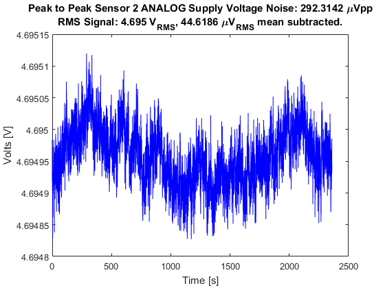
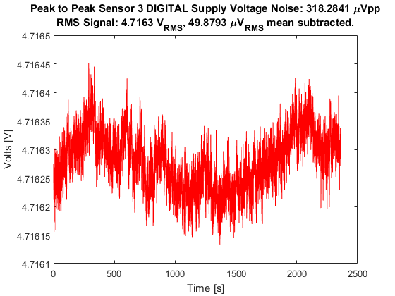
I am working on a temperature sensor design based on the ADS1262 using a 2 legged Wheatstone bridge.  I use my incoming supply (~+4.7V) for DVDD, AVDD and Vref (the Wheatstone source voltage).  I have different decoupling caps (both 1u) on the digital and analog supply pins.  Vref+ is AIN0, Vref- is AIN1, Vin+ is AIN2, Vin- is AIN3.  I have placed 1u X2Y caps on the across the Vin and Vref inputs.  All other inputs are unused and shorted to REFOUT.  I am using the internal oscillator.  I use a 4.7nF C0G cap between CAPP and CAPN.  I am using SPI communication with 47R resistors inline to CS, SCLK, DIN and DOUT/DRDY.  START is held to DVDD through a 47R.  RESET/PWDN is connected to DVDD.  I have a 1u cap to gnd from BYPASS.  I have a two layer board, the entire second layer is GND.

I am communicating with 3 such circuits using the same SPI bus.

Registers are set to:

POWER: 0x10. Internal ref disabled.

INTERFACE: 0x04. Status byte enabled, checksum bit disabled.

MODE0: 0x00. Continuous conversion, chop disabled, no delay.

MODE1: 0x80.  FIR filter

MODE2: 0x81.  PGA bypassed, gain 1, 5 Sa/s

INPMUX: 0x23. Vin+: AIN2, VIN-: AIN3

IDACMUX: 0xBB. IDAC1, IDAC2 No Connection.

IDACMAG: 0x00. IDAC1, IDAC2 Off.

REFMUX: 0x09. VrefP: AIN0, VrefN: AIN1.

TDACP: 0x00. No connection.

TDACN:0x00. No connection.

GPIOCON:0x00. None connected.

GPIODAT:0x00. Output (default).


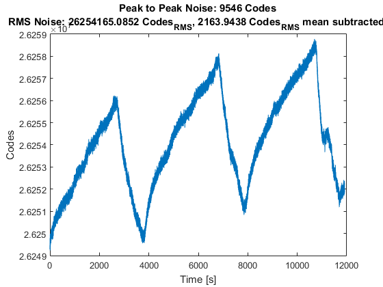
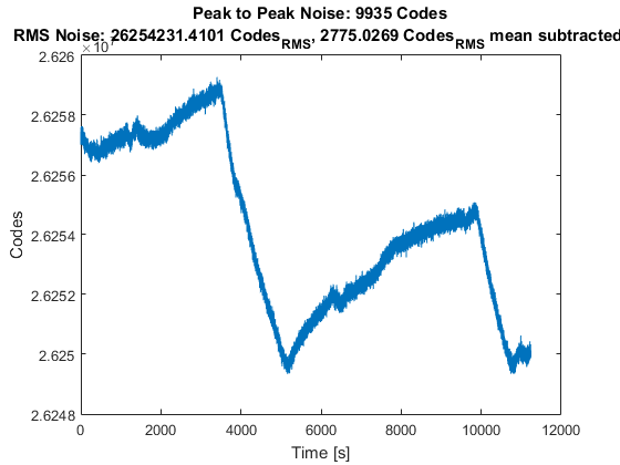
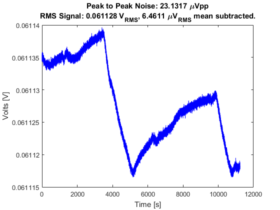
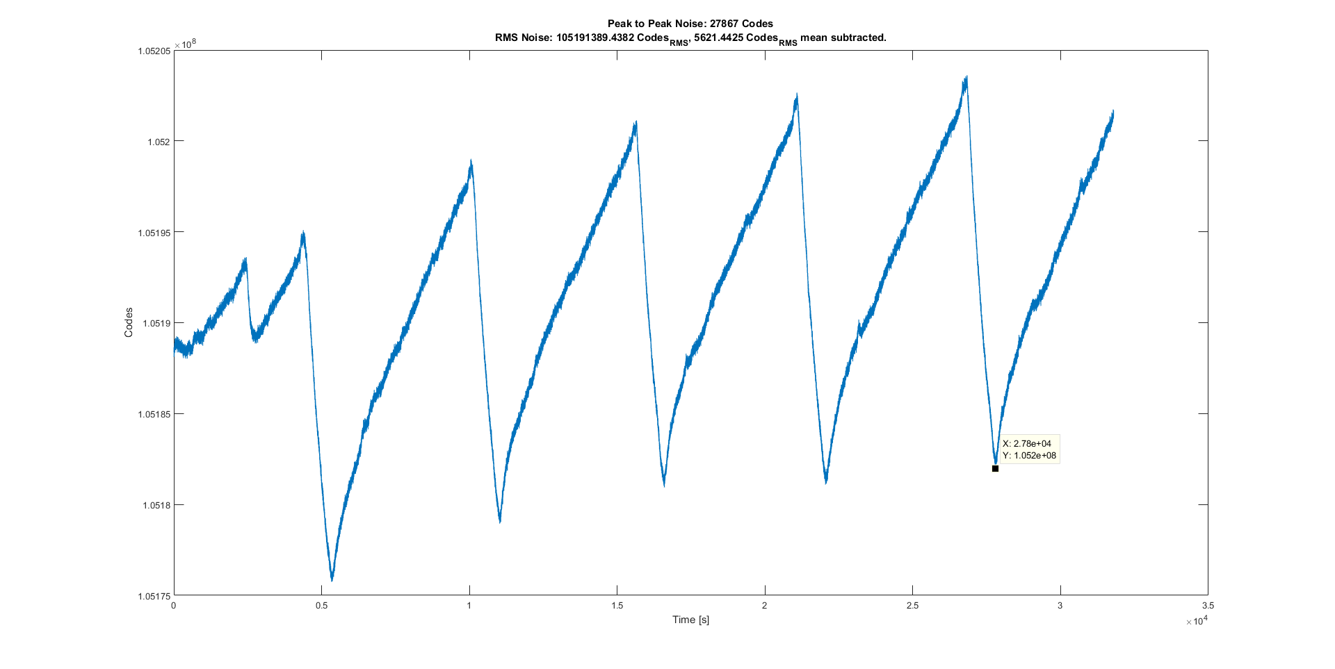
For my test experiment (to gather the attached data), I have replaced my temperature sensing elements with precision resistors (8k,+/- 0.01%, +/-0.2ppm/°C).  My fixed leg resistors are 8.2k (+/-0.1%,+/-10ppm/°C).  The goal is to establish my circuit's noise floor.  I am reading data by polling with a RDATA1 command every ~0.236s (a rate roughly 4.2Hz, so I am not quite getting all 5 samples however status byte is saying that data is new).  I am seeing a periodic charging and discharging with a time constant of ~1hr (4102s).  The magnitude of this charging is ~20uV.  It looks very much like some kind of R/L or RC periodic event but I can't identify the stimulus (must be some kind of square excitation). 

Please help!!


  • Hi Neal,

    Welcome to the TI E2E Forums!

    If I understand your circuit configuration correctly, you're measuring the bridge ratiometrically (VREF is used to excite the bridge), is that correct?

    Do you have any other components on your inputs (protection diodes, etc.) that might have some leakage current associated with them.?

    One thing that is standing out to me is the PGA bypassed setting. Is the common-mode voltage too close to one of the ADC supply rails that you need to bypass it? With an equivalent input impedance of about 8.1 kOhms, it would only require a change in bias (or leakage) current of about 2.5 nA to cause a 20 uV change in the voltage measurement. By enabling the PGA you would significantly reduce the input bias current to the ADC and perhaps resolve this issue.

    It would seem to me that the most likely cause is a differential input bias current that is drifting over time and/or temperature.

    Best regards,
    Chris
  • Hello Chris,

    Thanks for your reply!  

    No, I don't have any components on the inputs (other than the described).  No diodes or other.

    I wanted to use the PGA in its bypassed setting in order to have maximal temperature range.  I will redo the experiment tonight with it set to 1 to verify this hypothesis.  Could you please direct me to the section that describes the input bias current relationship?

    To me, it really seems as if there is some kind of power/decoupling/resonant or feedback mode that has been setup.  The waveform looks like a classic charging/discharging response to some step stimulus.  Not sure what would generate a stimulus/step threshold every hour or so though...  I initially suspected that the temperature of the resistors was causing some of this drift but given the specified drift values this seems like a stretch...

  • Sorry - in addition to my previous response: yes, I am measuring the bridge ratiometrically. Vref (ideally +5V) is used to excited the bridge.
  • No joy.  Ran similar experiments where I set the gain to 1 but enabled the PGA and a second set where I set the gain to 4 (PGA enabled obviously).  It seems to have changed the time constant but, perhaps surprisingly, not the peak 2 peak magnitude of the oscillation between the gain=1 PGA enabled vs. disabled case.  When gain is set to 4 the peak 2 peak oscillation magnitude decreased slightly.  To me, this really seems like some kind of feedback that is being setup.  Perhaps a supply or supply decoupling issue.  I should mention that I have not performed a calibration yet as I assumed that the calibration is simply a zeroth and first order adjustment and wouldn't effect transient, periodic effects such as what we're seeing.  Could I send you my layout/circuit diagram perhaps?  I am hoping that there is some kind of silly mistake there...

  • Hi Neal,

    For input bias current specifications, take a look at the "ADC1 ANALOG INPUTS" section on page 8, as well as figures 25 through 30, starting on page 16. You'll notice that figures 25 and 26 show much larger bias currents when the PGA is bypassed.

    Thanks for trying the test again with the PGA enabled! I had figured that the input bias current would be the mostly likely cause of the 20 uV offset, but if you still see it with the PGA enabled then I'd be inclined to look for other external causes. I'd also agree with you that calibration wouldn't change this behavior, it would only help to remove the initial offset.

    I'd be glad to look at your layout, feel free to send it to me via pa_deltasigma_apps@ti.com.

    A few other questions I have: 

    • Have you tried cleaning your boards? We've seen solder flux residue cause strange offset drifts before:


    • Is your resistor bridge on the same board as the ADC, or is it connected to the ADC via long wires? Long wires can act as antennas and pickup ambient noise or signals.
       
    • What is providing your 5V reference? Is it stable? Since you've configured your measurement ratiometrically, I would expect that your circuit would be fairly immune to any changes in the reference voltage. However, it is difficult to get 100% matching between the signal and reference inputs, so a change in the reference voltage may still have a small effect on the measurement.

    A few other troubleshooting other ideas...

    • As a sanity check, you could short the inputs together (connect both inputs to one side of the bridge) and measure the offset over time. If the offset is stable, then you know that the periodic offset is a real signal that is external to the ADC. 

    • You might also try removing the X2Y caps just to rule them out as a possible source of leakage current. Perhaps they could have been damaged during soldering.

    • If you have a large ESD bag, you could try placing your circuit in the bag and closing it up (as best you can). The bag can isolate the circuit from air currents, and if you ground the bag it will also act like a Faraday cage.


    Best regards,
    Chris

  • Hello Chris,

    Thank you very much for your insightful suggestions.  I have sent you my schematic and board layout, please let me know if you need anything else.  Regarding your suggestions:

    - We scrubbed the boards with alcohol after soldering and they look very clean under the microscope.  I will give it another go just to be certain.

    - The entire ADC circuit is on the same PCB with the same ground plane.

    - The 5V reference is questionable.  I assumed since it was a ratiometric configuration that I would gain some immunity but perhaps not.  I was wondering about this myself so I ran the following experiment: as  mentioned before, the sensor with the fixed resistors is on the same SPI bus as two other sensors (identical except they have thermistors in lieu of fixed precision resistors. BTW, they are also exhibiting nearly identical fluctuations, just much larger magnitude.)   I configured these extra sensors so that one read the analog voltage and the other read the digital voltage (relative each sensor's internal reference).  I have attached the figures generated.  Please note that this test is run simultaneously.  There is definitely some correlation between the oscillation measured on Sensor 1 and the voltage drift measured on the analog and digital voltages of sensors 2 and 3 respectively but it is hard for me to know how much source drift is acceptable....

    - Shorting the inputs seems like an excellent test.  How should I best do this?  Is there a way to do this internally to the chip by setting the MUX perhaps?

    - Good idea.  Was planning to start removing caps in general and retest.  Will do and send data.

    - Good idea.  Will do.

  • Hi Neal,

    I replied to your email with a couple of comments on the layout.

    It's very interesting that you're seeing a similar issue with your other sensors...Are you using the same supply/reference voltage for the other boards as well?


    For the shorted input test, you can simply configure the INPMUX register to select the same input for the MUXP and MUXN fields...

    ...For an internal short, I would select AINCOM as the input for both MUXP and MUXN and I would enable the level shifter on AINCOM (VBIAS) so that you have a proper the input common-mode voltage.

    ...For an external short, just select one side of your bridge. So connect both MUXP and MUXN to AIN1, for example.


    Best regards,
    Chris