This thread has been locked.

If you have a related question, please click the "Ask a related question" button in the top right corner. The newly created question will be automatically linked to this question.

DAC3174: Test plan using Altera Arria10 SoC Evaluation Board

Part Number: DAC3174
Other Parts Discussed in Thread: DAC3171, FMC-DAC-ADAPTER

I want to test the DAC3174 device using Arria10 SoC Evaluation Board.

My plan is using the following card for testing purpose (Until we'll get the real board):

Testing plan diagram:

Did I use the right cards for the specific component and whether it connects like the diagram above?

Thanks,

Michal

  • Michal,

    Do you still need help with this?

    Regards,

    Jim

  • Hi,

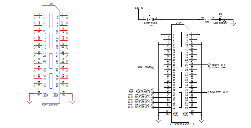
    To really answer the question I would strongly suggest comparing the connector pinout in the DAC3174 EVM schematics (attached) with the connector pinout of the FPGA board you wish to use.   You will have to do this anyway before you would be able to create your pin constraint file for your FPGA design, as you will need to know which FPGA pins are sourcing which signals to the DAC.   By tracing through all these signal paths from FPGA to DAC in advance then you would know for sure if the DAC EVM and FPGA card match up properly.   Back when we created the adapter boards to connect our ADC and DAC EVMs with the common FPGA platforms, we did not need to make an adapter board for the DAC EVMs to Altera because both boards used a common 3-segment Samtec connector.  But I am not familiar with the connector pinout on your specific FPGA board, so you would need to chase through all those signals from DAC to FPGA.

    Regards,

    Richard P.

    1715.DAC31X4EVM_B-SCH.pdf

  • Hello,

    We have now the DAC3174 EVM but as we see there is no FMC connector on it.

    Can we use the HSMC-FMC bridge (at ) to connect the DAC EVM to the Arria10 EVB?

    Also, I couldn't find the DAC3174 EVM schematics at the TI website. Is it the same schematic as attached above for DAC31x4 EVM?

    Thanks,

    Michal

  • Hi,

    no, that would not be the adapter card to bridge the DAC EVM to an FMC connector.   That bridge card you listed is the *ADC* to FMC adapter.  You would need the *DAC* to FMC adapter.   http://www.ti.com/tool/fmc-dac-adapter 

    Our LVDS ADC EVMs use a 2-segment Samtec connector.   Our LVDS DAC EVMs need more signals for the LVDS interface (such as the SYNC or ISTROBE signal) and thus use a 3-segment Samtec connector.   The design files for the DAC to FMC adapter are on that same web page for the adapter, and you would want to trace out which signals to the DAC EVM are connected to which FMC pins through the adapter so that you could know how to set up your pin constraints for the FPGA code. 

    The schematics for the DAC3174 EVM are attached.  It is not the same as the DAC3171 EVM.   Similar, but not the same.   The default option for output from the 2 channel EVM is through a complex modulator for the 2 channels, with solder options on some zero ohm resistors or AC coupling caps to steer the two channels directly to outputs instead of the modulator if desired.   For the 1 channel EVM, the complex modulator was not an option with just one channel so that EVM was a bit simpler.  The clocking and LVDS interface is the same between the two EVMs.

    Regards,

    Richard P.

    5861.DAC31X4EVM_B-SCH.pdf

  • Hello,

    My name is Timur, I'm working with Michal. I have a question according to DAC3147EVM and FMC-DAC-ADAPTER connectors. In 5861.DAC31X4EVM_B-SCH.pdf the connector has 180 pins and according to www.ti.com/.../fmc-dac-adapter the adapter has 160 pins in HSMC connector. How could it work?

    Thank you,
    Timur
  • Hi,

    the difference is that in one of those schematics a segment of the connector has the ground pins depopulated.  There are 20 gnd pins depopulated in the connector for the adapter board, but the adapter board also does not pass through any of the pins that the DAC EVM does have on that segment which are optional SPI control lines as well as an optional DAC reset and enable pin.   The DAC EVM has a DNI (do not install) on the signals for the DAC reset and enable from the connector, and the SPI lines are also not used on the DAC EVM.  So this segment of the Samtec connector is really not used anyway on the DAC EVM anyway, and the adapter board does not pass through any signals on this segment.   But the two connectors do mate with each other, even though one side is '160' pins and the other side is '180' pins.   Both have the spaces in the connector for 180 pins and match up properly.

    The segment on the right from the EVM starts with pins 1 3 5 down the left and 2 4 6 on the right.  The adapter card has blanks for pins 5 and 6.    Then the next 6 pins on the DAC are 7 9 11 down the left and 8 10 12 down the right.  The adapter card has blanks for pins 11 and 12, and the pins 7 8 9 10 are renumbered to 5 6 7 8.  That's all.

    Regards,

    Richard P.

  • PIN_ASSIGNMENT.xlsx

    Hi Richard,

    Thank you for detailed answer. I have another question regarding pinouts of the DAC and the ADAPTER. I'm mapping the pins to understand what  pins to define on FCM connector of the Arria 10 evaluation board. So, I encounter with some data pins on DAC HSMC connector, which in the same pin number on HSMC connector of the adapter are not  connected. I'm using the schematics of DAC3174 and HSMC2FMC given by you. Here are the problematic pins, in the table:

    DAC3174EVM HSMC (J14)  HSMC to FMC Header Adapter Card Arria10Soc EVB FMC
    Comments DACEVM Schematic name HSMC PIN HSMC PIN Adapter Schematic name FMC PIN FMC schematic name FPGA Schematic name FPGA PIN
      LED GREEN 1 1 N.C.        
      LED GREEN 2 2 N.C.        
      LED GREEN 3 3 N.C.        
      LED GREEN 4 4 N.C.        
      TXSP1 26 26 N.C.        
      TXEN 27 27 N.C.        
      TXSP2 28 28 N.C.        
      DAC_GPIO_0 45 45 N.C.        
      DAC_GPIO_3 51 51 N.C.        
      DAC_GPIO_6 57 57 N.C.        
      D12N 75 75 N.C.        
      DATACLKN 117 117 N.C.        
      FPGA_CLKOUTN 118 118 N.C.        
      D5N 123 123 N.C.        
      D4N 129 129 N.C.        
      D3N 135 135 N.C.        
      D2N 141 141 N.C.        
      D1N 147 147 N.C.        
      D0P 151 151 N.C.        
      D0N 153 153 N.C.        
      FIFO_ISTRP 176            
      FIFO_ISTRN 178            

    Best Regards,

    Timur

  • Hi,

    those signals you listed for pins 1 through 75 are on the first segment of the connector and are not passed through the FMC adapter, but they are not needed by the DAC EVM. 

    For signals in the remaining two segments, the signals you listed *are* passed through the adapter.  This is still all a part of your last question about one of the schematics listing 160 pins while the other lists 180 pins.   The schematics for the adapter omit 20 of the ground pins, and that throws off the pin numbering for the rest of the connector.   Take for example the signal DATACLK on pin 117 that you mention.   On the schematics for the adapter this pin number has become 97 because of those missing 20 ground pins.   but when you plug the EVM into the adapter that signal DATACLKN *is* present and passes through the adapter.  All of the necessary signals on the 2nd and 3rd segment of the connector do connect.   

    Regards,

    Richard P.

  • Hi,

    Now it is all clear, it looks fit, thank you very much!

    Best Regards,

    Timur

  • Hi George,

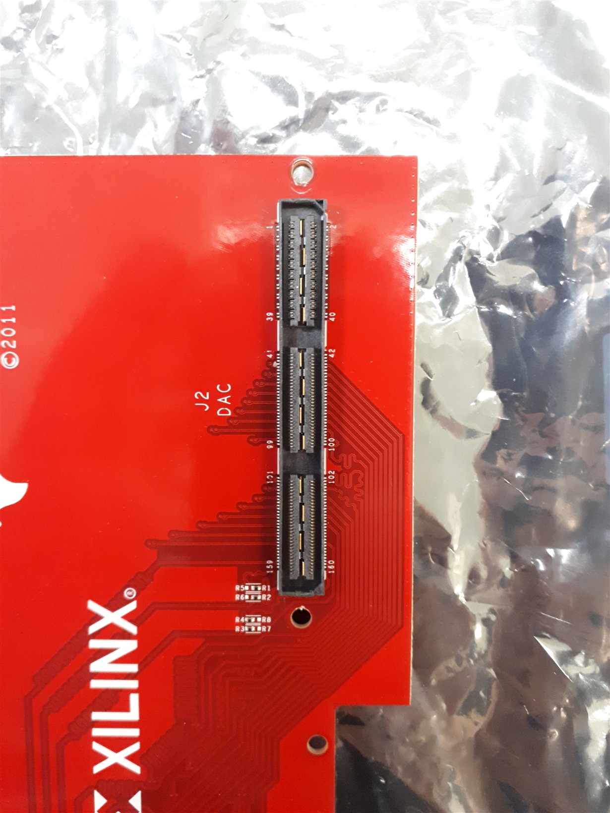
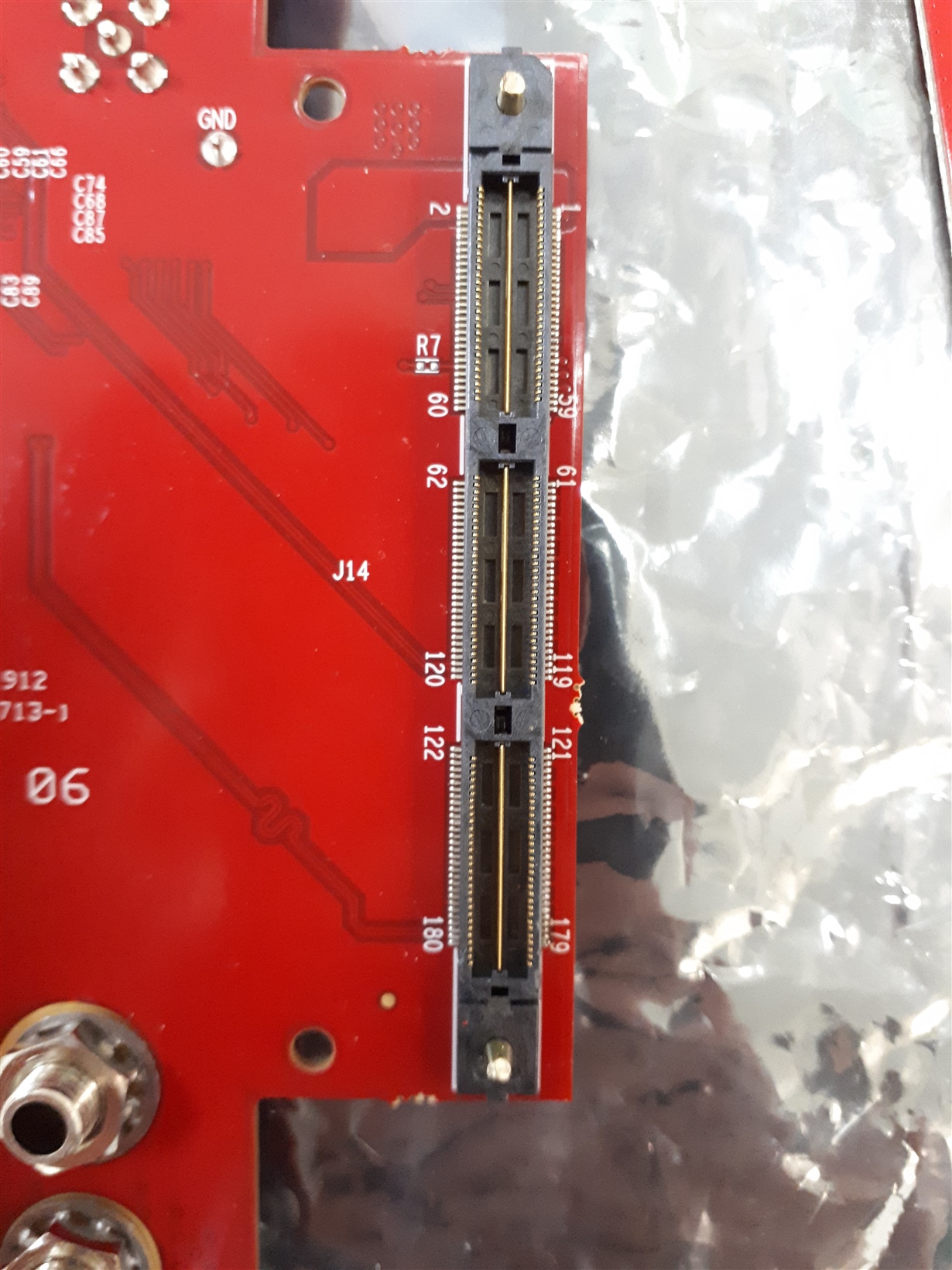
    We've got the adapter, but it doesn't connect smoothly to the DAC3174 board. I looked carefully at the both connectors of DAC 3174 and the adapter, the plastic part of the connecter is different.

    It seems to be, that the pins won't connect well or at all even if the plastic was fit exactly. 

    Pictures of both of them attached, first one- the adapter, second one - the DAC3174 board.

    What could be done about it?


    Best Regards,

    Timur Askerov

  • Ah, the EVM has gone to the locking connector from Samtec.  I was not expecting that issue.   Our DAC and ADC EVMs have been using these Samtec connectors for many years for the LVDS signals, and one issue with the original connectors was that there was nothing to hold them together, so often times while connecting SMA cables the EVM would pull away from the FPGA card.   To improve on that, Samtec added the posts to the connector that snap into the mating connector so that some force would be needed to pull them apart.   To some extent these two styles of connector were expected to be compatible, but if you look at the plastic housing on the one with posts you can see a little slant on the ends of the plastic around the outside segments and this prevents the EVM plastic from mating with the adapter plastic. 

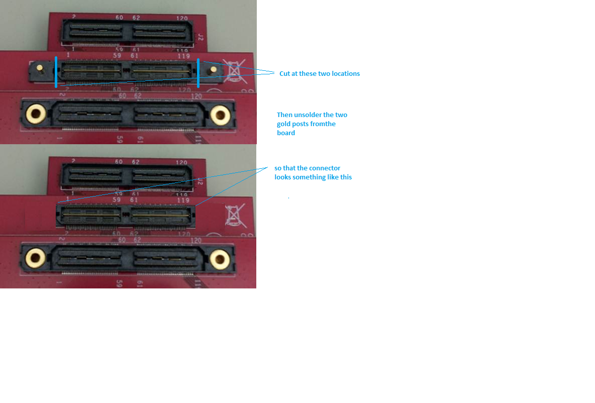
    We have seen this on occasion with a number of older EVMs.  What we have done on these occasions is to cut off the extra plastic on the connector with the posts.  We would take a fine saw blade (such as a hacksaw blade) and cut through the plastic outside the two end segments to remove that plastic sloping portion and cut down to the EVM and then unsolder the locking post.      an alternative is to unsolder the locking connector, and procure and solder downin its place the non-locking connector.  The is a wiki posting showing one of these at https://e2e.ti.com/support/data_converters/high_speed_data_converters/w/design_notes/3316.dac348x-hsmc-connectors?keyMatch=samtec%20connector%20locking%20post%20saw&tisearch=Search-EN-Everything 

    The easiest thing is to saw off the portion of the locking connector that is getting in the way.  You could do so yourself, or if you wish you could ship the adapter to us and we could make the modification and ship it back to you.  Attached is picture of where to cut the locking connector (using the 2 segment connector used on the ADCs rather than the 3 segment connector, but the concept is the same. The picture was just 'edited' to show the extra plastic removed which is why you don't see the holes where the posts would have been unsoldered.)

    Regards,

    Richard P.