This thread has been locked.

If you have a related question, please click the "Ask a related question" button in the top right corner. The newly created question will be automatically linked to this question.

ADS4249EVM: Interfacing ADS4249EVM with xilinx 7series FPGA "VC707"

Part Number: ADS4249EVM
Other Parts Discussed in Thread: ADS4249, , ADS5463

Hello Richard Prentice,

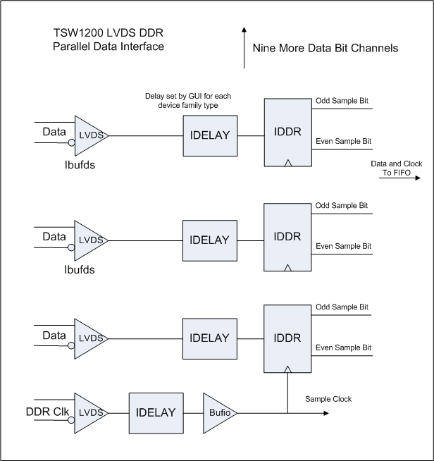
I am working on interfacing ADS4249EVM with xilinx 7series FPGA "VC707". I have received the clock and data from ADS4249 in VC707 according to the block diagram given below but skip the IDELAY portion. the data and clock is received in IBUFDS and IBUFGDS respectively and sent directly to IDDR and then route the output of IDDR (Q1 and Q2) to FPGA IO pins to see the result. 


The screen shot taken from an Oscilloscope is given below:

the blue signal in the above figure is the input differential clock from ADS4249EVM to IO pins of FPGA, the orange signal is the input double data rate signal from ADS4249 to IO pins of FPGA and the green signal is the output SDR signal from the IDDR which is routed to FPGA IO pins. The SDR data has both High and Low state at same time, which I am not getting.

Or it is necessary to use the IDELAY even slow sample rate i.e 10MHz

Thanks in anticipation.

Regards 

  • Hi,

    The fact that your oscilloscope shot shows both high and low data at the same time is because you are looking at a data stream of arbitrary data but telling your scope trace to 'trigger' at a location where the data goes from low to high, and you are looking at many such triggerings superimposed on top of one another.   The two bits right around your trigger are always low/high because that is your trigger condition, but the bits further away before and after the trigger may be sometimes low and sometimes high.  When you overlay many such triggerings you will see all these other bits with low on top of high.   If you switch your data pattern to a repetitive sample all the time then the display will not show the low on top of high like you have.

    That is a separate issue as to whether you need to use the IDELAY element or not.   To reliably capture the data correctly in the IDDR cell over the range of temperature and voltage and different part-to-part variations in timing among many such devices, then you need to know that you meet the setup and hold time of the data into the IDDR cell.   The static timing analysis tools that come with the FPGA tools will tell you that if you can get the timing constraint defined correctly that tells the FPGA tools what the min and max timings of the data from the ADC are relative to the data clock.   Maybe you can close timing without the IDELAY cell, but maybe not.  In our old TSW1200 design we had different input delays in the FPGA for the data than we did for the clock input and clock buffer, and I found that for an ADC such as ADS5463 that had the data clock edge-aligned with the data transitions, the extra delay of the clock buffering was almost perfect to close timing.  I only had to use two taps of the IDELAY on clock to make the timing perfect.  but that wasn't true for data from something like the ADS4249 which had the clock edge centered relative to the data bits.  There I had to use about 15 taps of the IDELAY to match the extra delay the clock input buffering introduced.  But you can't know that without the static timing analysis.   you wouldn't know how close your design might be from failing if the temperature were to increase by a few degrees or more, or if you got devices from a different manufacturing batch next time. 

    another way of knowing if you have the timing optimized would be to add the IDELAY to the design, but then test the design with different IDELAY tap settings until you see the data be incorrect due to setup/hold violations - sweep the IDELAY on clock and on data to find where things break, and then lock down your IDELAY settings to the mid-point between those extremes.  This is a second-best approach though, because it still does not tell you that the timing will be good at all boundary conditions of the data sheet timing specifications - only under the conditions that were present when the IDELAY sweeps were done.

    Regards,

    Richard P.

  • Thanks Richard for the detailed reply, I will analyze the timing constrain in deep and will let you know the result but now I am sharing the results that I have received on UART when I interface ADS4249EVM with VC707.

    00111100000010
    00111100000010
    00111100000000
    11111100000001
    11111100000011
    11111100000010
    11111100000011
    11111100000011
    11111100000011
    11111100000011
    11111100000011
    11111100000001
    11111100000011
    11111100000010
    11111100000000
    11111100000000
    11111100000000
    11111100000011
    11111100000010
    11111100000010
    11111100000010
    11111100000000
    11111100000010
    11111100000010
    11111100000011
    11111100000010
    11111100000011
    11111100000011
    11111100000001
    11111100000010
    11111100000000
    11111100000010
    11111100000011
    11111100000010
    11111100000011
    11111100000011
    11111100000010
    11111100000000
    11111100000011
    11111100000011
    11111100000001
    11111100000001
    11111100000011
    11111100000001
    11111100000000
    11111100000011
    11111100000010
    11111100000011
    11111100000010
    11111100000010
    11111100000001
    11111100000001
    11111100000011
    11111100000000
    11111100000000
    11111100001001
    11111100001001
    11111100000001
    11111100001011
    11111100000001
    11111100000011
    11111100001001
    11111100001001
    11111100001000
    11111100000011
    11111100001011
    11111100001011

    these are the 64 samples that I have received on UART. As you see the first 4 bits (A0, A1, A2, A3) keeps on changing but the remaining 10 bits remains constant. I have set the clock to 10Mhz and input signal is 1MHz(Sine wave). Is this the expected result or I am doing some thing wrong.

    and please give me your email address, I will also send you my code. 

    Thanks and Regards

  • In Addition to the above replay..

    The input signal is of 1V, and even if I have change it to 2V and frequency to 2Mhz, the last 10 bits remains the same.

  • sir, I am very much expecting yours guidance in this regards.
  • Hi,

    with a sample clock of 10MHz and an input of either 1MHz or 2MHz then you should see the output codes show a sine wave pattern of 5 to 10 samples per cycle of the input sine wave, obviously.   And the samples you are capturing do not show that.  At this point I would double check the setup of the EVM with a scope to make sure that you do see all the LVDS signals toggling, that the clock and analog input are getting to the ADC with enough amplitude and the right common mode voltage, and that you have the ADC mode of operation set correctly.   For 10Msps you need to have the ADC in low-speed mode.    Make sure that is set correctly please.

    And if still having trouble with the FPGA interface then use the test patterns from the ADC to help debug the FPGA code.   The test patterns for ramp and custom pattern are perhaps the most useful.   The custom pattern could be used to set the pattern to 00 0000 0000 0001 to see that you are catching the lsb in the right position, then pattern 00 0000 0000 0010, and so on.  This helps find issues such as having the polarity of the DDR clock backwards.   Then the ramp pattern is an arithmetic counting pattern. and when the FPGA is able to capture this pattern correctly you should have the ADC interface working by then.  We do not have the resources to review and debug your FPGA code if you were to send it.

    Regards,

    Richard P.

  • Thanks for the reply Richard..

    As I am not using IDELAY primitive can that cause the problem, if so can you guide me through IDELAYE2 primitive (for 7 series) as I am not getting its port description settings and tab value setting to incorporate the delay for Clock and Data received on VC707 Kit from ADS4249EVM through FMC adapter.

    Thanks and regards

  • Hi,

    we've not used the IDELAY2 primitive nor programmed the Virtex7 series for LVDS interface.  you would need to work with Xilinx on that.   Whether your trouble is related to timing or other coding issue, I would suggest again using the test patterns to debug getting the data latched into the FPGA correctly.

    Regards,

    Richard P.